SLVS047L November 1981 – January 2015 LM237 , LM337
PRODUCTION DATA.
- 1 Features
- 2 Applications
- 3 Description
- 4 Simplified Schematic
- 5 Revision History
- 6 Pin Configuration and Functions
- 7 Specifications
- 8 Detailed Description
- 9 Application and Implementation
- 10Power Supply Recommendations
- 11Layout
- 12Device and Documentation Support
- 13Mechanical, Packaging, and Orderable Information
Package Options
Mechanical Data (Package|Pins)
Thermal pad, mechanical data (Package|Pins)
Orderable Information
9 Application and Implementation
NOTE
Information in the following applications sections is not part of the TI component specification, and TI does not warrant its accuracy or completeness. TI’s customers are responsible for determining suitability of components for their purposes. Customers should validate and test their design implementation to confirm system functionality.
9.1 Application Information
9.1.1 General Configurations
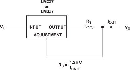 Figure 2. Current-Limiting Circuit
This application uses the LMx37 device's reference voltage, combined with the series resistor RS, to limit the current to 1.25 V ÷ RS
9.2 Typical Application
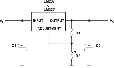 Figure 3. Adjustable Negative-Voltage Regulator
9.2.1 Design Requirements
- 1-µF solid tantalum on the input pin if the regulator is more than 10 cm from the power supply filter capacitor
- 1-µF solid tantalum or 10-µF aluminum electrolytic capacitor is required on the output pin for stability.
- R1, which is usually 120 Ω as part of the resistor divider.
- R2, which can be varied to change the value of VO.
9.2.2 Detailed Design Procedure
VO is determined by the values of R1 and R2. Choosing R1 = 120 Ω means that about 10.42 mA of current will flow through R1. The ~10 mA of current satisfies the minimum operating current and renders IREF negligible. Since the current is coming from ground, the same amount of current will flow through R2. Therefore, the size of R2 will be the dominant factor in adjusting VO. The relationship between R1, R2, and VO is as follows:
where
9.2.3 Application Curves
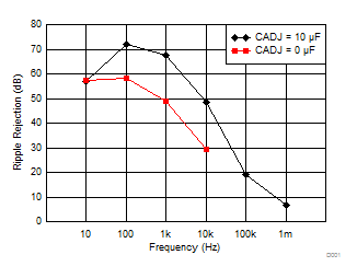 Figure 4. Ripple Rejection Over Frequency