SLVS047L November 1981 – January 2015 LM237 , LM337
PRODUCTION DATA.
- 1 Features
- 2 Applications
- 3 Description
- 4 Simplified Schematic
- 5 Revision History
- 6 Pin Configuration and Functions
- 7 Specifications
- 8 Detailed Description
- 9 Application and Implementation
- 10Power Supply Recommendations
- 11Layout
- 12Device and Documentation Support
- 13Mechanical, Packaging, and Orderable Information
Package Options
Mechanical Data (Package|Pins)
Thermal pad, mechanical data (Package|Pins)
Orderable Information
11 Layout
11.1 Layout Guidelines
Traces on the input and output pins should be thick enough to carry 1.5 A of current without violating thermal requirements of the device or the system. In addition, a 1-µF solid tantalum capacitor is required on the input pin if the regulator is more than 10 cm from the power supply filter capacitor. A 1-µF solid tantalum or 10-µF aluminum electrolytic capacitor is required on the output pin for stability.
11.2 Layout Example
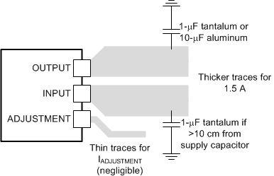 Figure 5. Layout Diagram