SNVS553C January 2008 – November 2016 LM3407
PRODUCTION DATA.
- 1 Features
- 2 Applications
- 3 Description
- 4 Revision History
- 5 Pin Configuration and Functions
- 6 Specifications
- 7 Detailed Description
- 8 Application and Implementation
- 9 Power Supply Recommendations
- 10Layout
- 11Device and Documentation Support
- 12Mechanical, Packaging, and Orderable Information
Package Options
Mechanical Data (Package|Pins)
- DGN|8
Thermal pad, mechanical data (Package|Pins)
- DGN|8
Orderable Information
7 Detailed Description
7.1 Overview
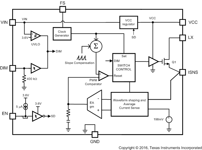
The LM3407 is a high power floating buck LED driver with a wide input voltage range. The device requires no loop compensation network. The integrated power N-MOSFET enables high-output power with up to 350-mA output current. The combination of Pulse Width Modulation (PWM), control architecture, and the proprietary Pulse Level Modulation (PLM) ensures accurate current regulation, good EMI performance, and provides high flexibility on inductor selection. High-speed dimming control input allows precision and high resolution brightness control for applications require fine brightness adjustment.
7.2 Functional Block Diagram
7.3 Feature Description
7.3.1 Floating Buck Switching Converter
The LM3407 is designed for floating buck configuration. Different from conventional buck converters, a low-side power N-MOSFET is used. The floating buck configuration simplifies the driver stage design and reduces the die size of the power MOSFET. Additionally, the connections of the power diode, inductor and output capacitor are switched to ground with a ground referenced power switch, Q1. The extraction of inductor current information can be easily realized by a simple current sensing resistor. These benefits combine to provide a high efficiency, low cost, and reliable solution for LED lighting applications.
The operation of the LM3407 constant current output floating buck converter is explained below. With the internal switch Q1 turned ON, current flows through the inductor L1 and the LED array. Energy is also stored in the magnetic field of the inductor during the ON cycle. The current flowing through RISNS during the ON cycle is monitored by the Average Current Sensing block. The switch will remain ON until the average inductor current equals 198 mV / RISNS. When the switch is turned OFF, the magnetic field starts to collapse and the polarity of the inductor voltage reverses. At the same time, the diode is forward biased and current flows through the LED, releasing the energy stored in the inductor to the output. True average output current is achieved as the switching cycle continuously repeats and the Average Current Sensing block controls the ON duty cycle. A constant current output floating buck converter only works in Continuous Conduction Mode (CCM); if the converter enters Discontinuous Conduction Mode (DCM) operation, the current regulation will deteriorate and the accuracy of LED current cannot be maintained. The operating waveforms for the typical application circuit are shown in Figure 18.
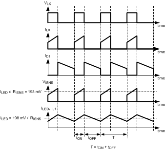 Figure 18. Operating Waveforms of a Floating Buck Converter
7.3.2 Pulse Level Modulation (PLM)
The LM3407 incorporates the innovative Pulse Level Modulation technique. With an external 1% thick film resistor connected to the ISNS pin, the converter output voltage can adjust automatically as needed to deliver constant current within 10% accuracy to a serially connected LED string of different number and type. Pulse Level Modulation is a novel method to provide precise constant current control with high efficiency. It allows the use of low side current sensing and facilitates true average output current regulation regardless of the input voltage and inductor value. Pulse Level Modulation can be treated as a process that transforms a trapezoidal pulse chain into a square pulse chain with an amplitude equal to the center of inductor current ramp. Figure 19 shows the waveform of the converter in steady state. In the figure, IL1 is the inductor current and ILX is the switch current into the LX pin. VISNS is the voltage drop across the current sensing resistor RISNS. VMSL is the center of the inductor current ramp and is a reference pulse that is synchronized and has an identical pulse width to VISNS.
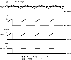 Figure 19. LM3407 Switching Waveforms
The switching frequency and duty ratio of the converter equal:

By comparing the area of VISNS and VRP over the ON period, an error signal is generated. Such a comparison is functionally equivalent to comparing the middle level of ISNS to VRP during the ON-period of a switching cycle. The error signal is fed to a PWM comparator circuit to produce the PWM control pulse to drive the internal power N-MOSFET. Figure 20 shows the implementation of the PWM switching signal. The error signal is fed to a PWM comparator circuit to produce the PWM control pulse to drive the internal power N-MOSFET. Figure 20 shows the implementation of the PWM switching signal.
In closed-loop operation, the difference between VMSL and VRP is reflected in the changes of the switching duty cycle of the power switch. This behavior is independent of the inductance of the inductor and input voltage because for the same set of IOUT * RISNS, ON time, and switching period, there exists only one VMSL. Figure 21 shows two sets of current sense signals named VISNS1 and VISNS2 that have identical frequencies and duty cycles but different shapes of trapezoidal waveforms, each generating identical PWM signals.
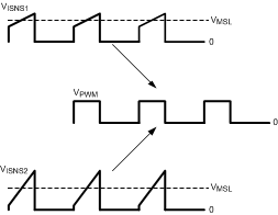 Figure 20. Pulse-Level Transformation
When VMSL is higher than VREF, the peak value of VRP, the switching duty cycle of the power switch will be reduced to lower VMSL. When VMSL is lower than the peak value of VRP, the switching duty cycle of the power switch will be increased to raise VMSL. For example, when IOUT is decreased, VMSL will become lower than VREF. In order to maintain output current regulation, the switching duty cycle of the power switch will be increased and eventually push up VMSL until VMSL equals VREF. Because in typical floating buck regulators VMSL is equal to IOUT × RISNS, true average output current regulation can be achieved by regulating VMSL. Figure 22 shows the waveforms of VISNS and VRP under closed loop operation.
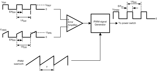 Figure 21. Implementation of the PWM Switching Signal
 Figure 22. Waveforms of VISNS and VRP Under Closed-Loop Operation
7.3.3 Internal VCC Regulator
The LM3407 has an internal 4.5 V linear regulator. This regulated voltage is used for powering the internal circuitry only and any external loading at the VCC pin is not recommended. The supply input (VIN) can be connected directly to an input voltage up to 30 V. The VCC pin provides voltage regulated at 4.5 V for VIN ≤ 6 V. For 4.5 V ≤ VIN ≤ 6 V, VIN pin will be connected to VCC pin directly by an internal bypassing switch. For stability reason, an external capacitor CVCC with at least 680 nF (1 µF recommended) must be connected to the VCC pin.
7.3.4 Clock Generator
The LM3407 features an integrated clock generator to control the switching frequency of the converter, fSW. An external resistor RFS, connected to the FS pin and ground, determines the switching frequency. The oscillator frequency can be set in the range of 300 kHz to 1 MHz. The relationship between the frequency setting resistance and the oscillator frequency is described in the Application Information Section.
7.3.5 PWM Dimming of LED String
Dimming of LED brightness is achieved by Pulse Width Modulation (PWM) control of the LED current. Pulse Width Modulation control allows LED brightness to be adjusted while still maintaining accurate LED color temperature. The LM3407 accepts an external PWM dimming signal at the DIM pin. The signal is buffered before being applied to the internal switch control block responsible for controlling the ON/OFF of the power switch, Q1. The DIM pin is internally pulled low by a resistor and no LED current will be available when the DIM pin is floating or shorted to ground. Functionally, the DIM pin can also be used as an external device disable control. Device switching will be disabled if the DIM pin is not connected or tied to ground.
7.3.6 Input Under-Voltage Lock-Out (UVLO)
The LM3407 incorporates an input Under-Voltage Lock-Out (UVLO) circuit with hysteresis to keep the device disabled when the input voltage (VIN) falls below the Lock-Out Low threshold, 3.4 V typical. During the device power-up, internal circuits are held inactive and the UVLO comparator monitors the voltage level at the VIN pin continuously. When the VIN pin voltage exceeds the UVLO threshold, 3.6 V typical, the internal circuits are then enabled and normal operation begins.
7.4 Device Functional Modes
7.4.1 Low-Power Shutdown Mode
The LM3407 comes with a dedicated device enable pin, EN, for low-power shutdown of the device. By putting the device in shutdown mode, most of the internal circuits will be disabled and the input current will reduced to below typically 50 µA. The EN pin is internally pulled high by a 5-µA current source. Connecting the EN pin to ground will force the device to enter low power shutdown mode. To resume normal operation, leave the EN pin open or drive with a logic high voltage.