SNVS553C January 2008 – November 2016 LM3407
PRODUCTION DATA.
- 1 Features
- 2 Applications
- 3 Description
- 4 Revision History
- 5 Pin Configuration and Functions
- 6 Specifications
- 7 Detailed Description
- 8 Application and Implementation
- 9 Power Supply Recommendations
- 10Layout
- 11Device and Documentation Support
- 12Mechanical, Packaging, and Orderable Information
Package Options
Mechanical Data (Package|Pins)
- DGN|8
Thermal pad, mechanical data (Package|Pins)
- DGN|8
Orderable Information
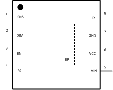
5 Pin Configuration and Functions
DGN Package
8-Pin MSOP
Top View

Pin Functions
| PIN | I/O | DESCRIPTION | |
|---|---|---|---|
| NO. | NAME | ||
| 1 | ISNS | I | Connect resistor RISNS from this pin to ground for LED current sensing. The current sensing resistor should be placed close to this pin. |
| 2 | DIM | I | PWM Dimming Control Pin. Applying a logic level PWM signal to this pin controls the intended brightness of the LED string. |
| 3 | EN | I | Applying logic high to this pin or leaving it open enables the switcher. When pulled low the switcher is disabled and will enter low power shutdown mode. |
| 4 | FS | I | Switching Frequency Setting Pin. Connect resistor RFS from this pin to ground to set the switching frequency. |
| 5 | VIN | I | Input Voltage Pin. The input voltage should be in the range of 4.5 V to 30 V |
| 6 | VCC | O | Internal Regulator Output Pin. This pin should be bypassed to ground by a ceramic capacitor with a minimum value of 1 µF. |
| 7 | GND | — | This pin should be connected to the system ground. |
| 8 | LX | O | Drain of N-MOSFET Switch. Connect this pin to the output inductor and anode of the Schottky diode. |
| EP | EP | — | Thermal Pad (Power Ground). Used to dissipate heat from the package during operation. Must be electrically connected to GND external to the package. |