SNVSCL9B March 2011 – December 2024 LM3481-Q1
PRODUCTION DATA
- 1
- 1 Features
- 2 Applications
- 3 Description
- 4 Pin Configuration and Functions
- 5 Specifications
- 6 Detailed Description
-
7 Application and Implementation
- 7.1 Application Information
- 7.2
Typical Applications
- 7.2.1
Boost Converter
- 7.2.1.1 Design Requirements
- 7.2.1.2
Detailed Design Procedure
- 7.2.1.2.1 Custom Design with WEBENCH Tools
- 7.2.1.2.2 Power Inductor Selection
- 7.2.1.2.3 Programming the Output Voltage and Output Current
- 7.2.1.2.4 Current Limit With Additional Slope Compensation
- 7.2.1.2.5 Power Diode Selection
- 7.2.1.2.6 Power MOSFET Selection
- 7.2.1.2.7 Input Capacitor Selection
- 7.2.1.2.8 Output Capacitor Selection
- 7.2.1.2.9 Driver Supply Capacitor Selection
- 7.2.1.2.10 Compensation
- 7.2.1.3 Application Curve
- 7.2.2 Typical SEPIC Converter
- 7.2.1
Boost Converter
- 7.3 Power Supply Recommendations
- 7.4 Layout
- 8 Device and Documentation Support
- 9 Revision History
- 10Mechanical, Packaging, and Orderable Information
Package Options
Mechanical Data (Package|Pins)
- DGS|10
Thermal pad, mechanical data (Package|Pins)
Orderable Information
7.2.1.2.6 Power MOSFET Selection
The drive pin, DR, of the LM3481-Q1 must be connected to the gate of an external MOSFET. In a boost topology, the drain of the external N-Channel MOSFET is connected to the inductor and the source is connected to the ground. The drive pin voltage, VDR, depends on the input voltage (see Section 5.6). In most applications, a logic level MOSFET can be used. For very low input voltages, a sub-logic level MOSFET should be used.
The selected MOSFET directly controls the efficiency. The critical parameters for selection of a MOSFET are:
- Minimum threshold voltage, VTH(MIN)
- On-resistance, RDS(ON)
- Total gate charge, Qg
- Reverse transfer capacitance, CRSS
- Maximum drain to source voltage, VDS(MAX)
The off-state voltage of the MOSFET is approximately equal to the output voltage. VDS(MAX) of the MOSFET must be greater than the output voltage. The power losses in the MOSFET can be categorized into conduction losses and ac switching or transition losses. RDS(ON) is needed to estimate the conduction losses. The conduction loss, PCOND, is the I2R loss across the MOSFET. The maximum conduction loss is given by:
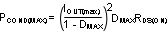
where DMAX is the maximum duty cycle.

At high switching frequencies the switching losses may be the largest portion of the total losses.
The switching losses are very difficult to calculate due to changing parasitics of a given MOSFET in operation. Often, the individual MOSFET datasheet does not give enough information to yield a useful result. Equation 38 and Equation 39 give a rough idea how the switching losses are calculated:

