SNVS653E July 2011 – August 2015 LM3532
PRODUCTION DATA.
- 1 Features
- 2 Applications
- 3 Description
- 4 Revision History
- 5 Pin Configuration and Functions
- 6 Specifications
-
7 Detailed Description
- 7.1 Overview
- 7.2 Functional Block Diagram
- 7.3 Feature Description
- 7.4
Device Functional Modes
- 7.4.1 LED Current Ramping
- 7.4.2 Start-up and Shutdown Current Ramping
- 7.4.3 Run-Time Ramp Rates
- 7.4.4 LED Current Mapping Modes
- 7.4.5 Exponential Current Mapping Mode
- 7.4.6 Linear Current Mapping
- 7.4.7 LED Current Control
- 7.4.8 Assigning and Enabling a PWM Input
- 7.4.9 Enabling a Current Sink
- 7.4.10
Ambient Light Sensor Current Control
- 7.4.10.1 ALS Resistors
- 7.4.10.2 Ambient Light Zone Boundaries
- 7.4.10.3 Ambient Light Zone Hysteresis
- 7.4.10.4 PWM Enabled for a Particular Zone
- 7.4.10.5 ALS Operation
- 7.4.10.6 ALS Input Select and ALS ADC Input
- 7.4.10.7 ALS ADC Readback
- 7.4.10.8 ALS Averaging
- 7.4.10.9 ALS ADC Average Readback
- 7.4.10.10 Initializing the ALS
- 7.4.10.11 ALS Operation
- 7.4.10.12 Direct ALS Control
- 7.4.11 Down Delay
- 7.5 Programming
- 7.6
Register Maps
- 7.6.1 Output Configuration
- 7.6.2 Start-up/Shutdown Ramp Rate
- 7.6.3 Run-Time Ramp Rate
- 7.6.4 Control A PWM
- 7.6.5 Control B PWM
- 7.6.6 Control C PWM
- 7.6.7 Control A Brightness Configuration
- 7.6.8 Control B Brightness Configuration
- 7.6.9 Control C Brightness Configuration
- 7.6.10 Control A, B, and C Full-Scale Current
- 7.6.11 Feedback Enable
- 7.6.12 Control Enable
- 7.6.13 ALS1 and ALS2 Resistor Select
- 7.6.14 ALS Down Delay
- 7.6.15 ALS Configuration
- 7.6.16 ALS Zone Readback / Information
- 7.6.17 ALS Zone Boundaries
- 7.6.18 Zone Target Registers
- 8 Application and Implementation
- 9 Power Supply Recommendations
- 10Layout
- 11Device and Documentation Support
- 12Mechanical, Packaging, and Orderable Information
Package Options
Mechanical Data (Package|Pins)
- YFQ|16
Thermal pad, mechanical data (Package|Pins)
Orderable Information
8 Application and Implementation
NOTE
Information in the following applications sections is not part of the TI component specification, and TI does not warrant its accuracy or completeness. TI’s customers are responsible for determining suitability of components for their purposes. Customers should validate and test their design implementation to confirm system functionality.
8.1 Application Information
The LM3532 incorporates a 40-V (maximum output) boost, three high-voltage, low-side current sinks, and programmable dual ambient light sensor inputs with internal-sensor gain selection. The device can drive up to 3 parallel high-voltage LED strings with up to 90% efficiency. The adaptive current regulation method allows for different LED currents in each current sink, thus allowing for a wide variety of backlight-with-keypad applications.
8.2 Typical Application
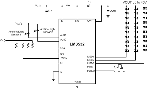 Figure 23. LM3532 Typical Application
8.2.1 Design Requirements
For typical white LED applications, use the parameters listed in Table 20:
Table 20. Design Parameters
| DESIGN PARAMETER | EXAMPLE VALUE |
|---|---|
| Input voltage range | 2.7 V to 5.5 V |
| Output current | 500 MHz typical |
| Boost switching frequency | 2 MHz |
8.2.2 Detailed Design Procedure
Table 21. Suggested Application Circuit Component List
| COMPONENT | MANUFACTURER'S PART NUMBER | VALUE | SIZE | CURRENT/VOLTAGE RATING (RESISTANCE) |
|---|---|---|---|---|
| L | COILCRAFT LPS4018-103ML |
10 µH | 3.9 mm x 3.9 mm x 1.7 mm | 1 A (RDC = 0.2 Ω) |
| COUT | Murata GRM21BR71H105KA12L |
1 µF | 0805 | 50 V |
| CIN | Murata GRM188R71A225KE15D |
2.2 µF | 0603 | 10 V |
8.2.2.1 Inductor Selection
The LM3532 is designed to work with a 10-µH to 22-µH inductor. When selecting the inductor, ensure that the saturation rating is high enough to accommodate the applications peak inductor current . The inductance value must also be large enough so that the peak inductor current is kept below the LM3532's switch current limit. See Maximum Output Power for more details. Table 22 lists various inductors that can be used with the LM3532. The inductors with higher saturation currents are more suitable for applications with higher output currents or voltages (multiple strings). The smaller devices are geared toward single string applications with lower series LED counts.
Table 22. Suggested Inductors
| MANUFACTURER | PART NUMBER | VALUE | SIZE | CURRENT RATING | DC RESISTANCE |
|---|---|---|---|---|---|
| TDK | VLS252010T-100M | 10 µH | 2.5 mm × 2 mm × 1 mm | 590 mA | 0.712 Ω |
| TDK | VLS2012ET-100M | 10 µH | 2 mm × 2 mm × 1.2 mm | 695 mA | 0.47 Ω |
| TDK | VLF301512MT-100M | 10 µH | 3.0 mm × 2.5 mm × 1.2mm | 690 mA | 0.25 Ω |
| TDK | VLF4010ST-100MR80 | 10 µH | 2.8 mm × 3 mm × 1 mm | 800 mA | 0.25 Ω |
| TDK | VLS252012T-100M | 10 µH | 2.5 mm × 2 mm × 1.2mm | 810 mA | 0.63 Ω |
| TDK | VLF3014ST-100MR82 | 10 µH | 2.8 mm × 3 mm × 1.4mm | 820 mA | 0.25 Ω |
| TDK | VLF4014ST-100M1R0 | 10 µH | 3.8 mm × 3.6 mm × 1.4 mm | 1000 mA | 0.22 Ω |
| Coilcraft | XPL2010-103ML | 10 µH | 1.9 mm × 2 mm × 1 mm | 610 mA | 0.56 Ω |
| Coilcraft | LPS3010-103ML | 10 µH | 2.95 mm × 2.95 mm × 0.9 mm | 550 mA | 0.54 Ω |
| Coilcraft | LPS4012-103ML | 10 µH | 3.9mm × 3.9mm × 1.1mm | 1000 mA | 0.35 Ω |
| Coilcraft | LPS4012-223ML | 22 µH | 3.9 mm × 3.9 mm × 1.1 mm | 780 mA | 0.6 Ω |
| Coilcraft | LPS4018-103ML | 10 µH | 3.9 mm × 3.9 mm × 1.7 mm | 1100 mA | 0.2 Ω |
| Coilcraft | LPS4018-223ML | 22 µH | 3.9 mm × 3.9 mm × 1.7 mm | 700 mA | 0.36 Ω |
8.2.2.2 Capacitor Selection
The LM3532’s output capacitor has two functions: filtering of the boost converter's switching ripple, and to ensure feedback loop stability. As a filter, the output capacitor supplies the LED current during the boost converter's on time and absorbs the inductor's energy during the switch's off time. This causes a sag in the output voltage during the on time and a rise in the output voltage during the off time. Because of this, the output capacitor must be sized large enough to filter the inductor current ripple that could cause the output voltage ripple to become excessive. As a feedback loop component, the output capacitor must be at least 1µF and have low ESR; otherwise, the LM3532's boost converter can become unstable. This requires the use of ceramic output capacitors. Table 23 lists part numbers and voltage ratings for different output capacitors that can be used with the LM3532.
Table 23. Input/Output Capacitors
| MANUFACTURER | PART NUMBER | VALUE | SIZE | RATING | DESCRIPTION |
|---|---|---|---|---|---|
| Murata | GRM21BR71H105KA12 | 1 µF | 0805 | 50 V | COUT |
| Murata | GRM188B31A225KE33 | 2.2 µF | 0805 | 10 V | CIN |
| TDK | C1608X5R0J225 | 2.2 µF | 0603 | 6.3 V | CIN |
8.2.2.3 Diode Selection
The diode connected between the SW and OUT pins must be a Schottky diode and have a reverse breakdown voltage high enough to handle the maximum output voltage in the application. Table 24 lists various diodes that can be used with the LM3532.
Table 24. Diodes
| MANUFACTURER | PART NUMBER | VALUE | SIZE | RATING |
|---|---|---|---|---|
| Diodes Inc. | B0540WS | Schottky | SOD-323 | 40/500 V/mA |
| Diodes Inc. | SDM20U40 | Schottky | SOD-523 (1.2 mm × 0.8 mm × 0.6 mm) | 40/200 V/mA |
| On Semiconductor | NSR0340V2T1G | Schottky | SOD-523 (1.2 mm × 0.8 mm × 0.6 mm) | 40/250 V/mA |
| On Semiconductor | NSR0240V2T1G | Schottky | SOD-523 (1.2 mm × 0.8 mm × 0.6 mm) | 40/250 V/mA |
8.2.2.4 Maximum Output Power
The LM3532 device's maximum output power is governed by two factors: the peak current limit (ICL = 880 mA minimum), and the maximum output voltage (VOVP = 40 V minimum). When the application causes either of these limits to be reached it is possible that the proper current regulation and matching between LED current strings may not be met.
8.2.2.4.1 Peak Current Limited
In the case of a peak current limited situation, when the peak of the inductor current hits the LM3532's current limit the NFET switch turns off for the remainder of the switching period. If this happens, each switching cycle the LM3532 begins to regulate the peak of the inductor current instead of the headroom across the current sinks. This can result in the dropout of the feedback-enabled current sinks and the current dropping below its programmed level.
The peak current in a boost converter is dependent on the value of the inductor, total LED current (IOUT), the output voltage (VOUT) (which is the highest voltage LED string + 0.4 V regulated headroom voltage), the input voltage VIN, and the efficiency (output power/input power). Additionally, the peak current is different depending on whether the inductor current is continuous during the entire switching period (CCM) or discontinuous (DCM) where it goes to 0 before the switching period ends.
For CCM the peak inductor current is given by:

For DCM the peak inductor current is given by:

To determine which mode the circuit is operating in (CCM or DCM) it is necessary to perform a calculation to test whether the inductor current ripple is less than the anticipated input current (IIN). If ΔIL is < then IIN then the device is operating in CCM. If ΔIL is > IIN then the device is operating in DCM.

Typically at currents high enough to reach the LM3532's peak current limit, the device is operating in CCM.
Figure 24, Figure 25, Figure 26, and Figure 27 show the output current and voltage derating for a 10-µH and a 22-µH inductor. These plots take Equation 5 and Equation 6 from above and plot VOUT and IOUT with varying VIN, a constant peak current of 880 mA (ICL min), and a constant efficiency of 85%. Using these curves can give a good design guideline on selecting the correct inductor for a given output power requirement. A 10 µH is typically a smaller device with lower on resistance, but the peak currents are higher. A 22-µH inductor provides for lower peak currents, but to match the DC resistance of a 10-µH inductor requires a larger-sized device.
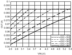 Figure 24. Maximum Output Power (22 µH)
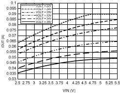 Figure 26. Maximum Output Power (10 µH)
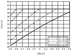 Figure 25. Maximum Output Power (22 µH)
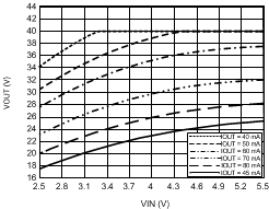 Figure 27. Maximum Output Power (10 µH)
8.2.2.4.2 Output Voltage Limited
When the LM3532 output voltage (highest voltage LED string + 400-mV headroom voltage) reaches 40 V, the OVP threshold is hit, and the NFET turns off and remains off until the output voltage drops 1V below the OVP threshold. Once VOUT falls below this hysteresis, the boost converter turns on again. In high output voltage situations the LM3532 begins to regulate the output voltage to the VOVP level instead of the current sink headroom voltage. This can result in a loss of headroom voltage across the feedback enabled current sinks resulting in the LED current dropping below its programmed level.
8.2.3 Application Curves
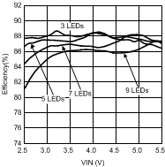
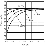
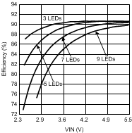
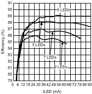
VIN = 3.6 V, LEDs (VF = 3.2 V at 20 mA, TA = 25°C), COUT = 1 µF, CIN = 2.2 µF, L = Coilcraft LPS4018-103ML (10 µH ) or LPS4018-223M (22 µH), TA = 25°C unless otherwise specified.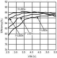
| ILED = 20.2 mA | L = 10 µH | |
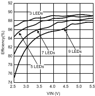
| ILED = 20.2 mA | L = 10 µH | |
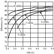
| ILED = 20.2 mA | L = 10 µH | |
| ILED = 20.2 mA | L = 22 µH | |
| ILED = 20.2 mA | L = 22 µH | |
| ILED = 20.2 mA | L = 22 µH | |
| VIN = 3.6 V | L = 10 µH | |
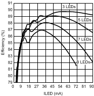
| VIN = 3.6 V | L = 22 µH | |
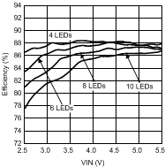
| ILED = 20.2 mA | L = 10 µH | |
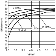
| ILED = 20.2 mA | L = 10 µH | |
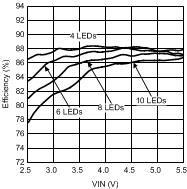
| ILED = 20.2 mA | L = 10 µH | |
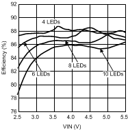
| ILED = 20.2 mA | L = 22 µH | |
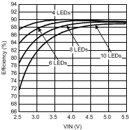
| ILED = 20.2 mA | L = 22 µH | |
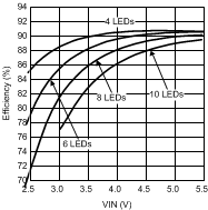
| ILED = 20.2 mA | L = 22 µH | |
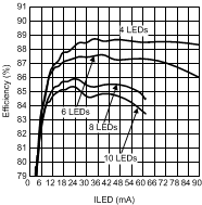
| VIN = 3.6 V | L = 10 µH | |
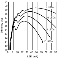
| VIN = 3.6 V | L = 22 µH | |