SNVS653E July 2011 – August 2015 LM3532
PRODUCTION DATA.
- 1 Features
- 2 Applications
- 3 Description
- 4 Revision History
- 5 Pin Configuration and Functions
- 6 Specifications
-
7 Detailed Description
- 7.1 Overview
- 7.2 Functional Block Diagram
- 7.3 Feature Description
- 7.4
Device Functional Modes
- 7.4.1 LED Current Ramping
- 7.4.2 Start-up and Shutdown Current Ramping
- 7.4.3 Run-Time Ramp Rates
- 7.4.4 LED Current Mapping Modes
- 7.4.5 Exponential Current Mapping Mode
- 7.4.6 Linear Current Mapping
- 7.4.7 LED Current Control
- 7.4.8 Assigning and Enabling a PWM Input
- 7.4.9 Enabling a Current Sink
- 7.4.10
Ambient Light Sensor Current Control
- 7.4.10.1 ALS Resistors
- 7.4.10.2 Ambient Light Zone Boundaries
- 7.4.10.3 Ambient Light Zone Hysteresis
- 7.4.10.4 PWM Enabled for a Particular Zone
- 7.4.10.5 ALS Operation
- 7.4.10.6 ALS Input Select and ALS ADC Input
- 7.4.10.7 ALS ADC Readback
- 7.4.10.8 ALS Averaging
- 7.4.10.9 ALS ADC Average Readback
- 7.4.10.10 Initializing the ALS
- 7.4.10.11 ALS Operation
- 7.4.10.12 Direct ALS Control
- 7.4.11 Down Delay
- 7.5 Programming
- 7.6
Register Maps
- 7.6.1 Output Configuration
- 7.6.2 Start-up/Shutdown Ramp Rate
- 7.6.3 Run-Time Ramp Rate
- 7.6.4 Control A PWM
- 7.6.5 Control B PWM
- 7.6.6 Control C PWM
- 7.6.7 Control A Brightness Configuration
- 7.6.8 Control B Brightness Configuration
- 7.6.9 Control C Brightness Configuration
- 7.6.10 Control A, B, and C Full-Scale Current
- 7.6.11 Feedback Enable
- 7.6.12 Control Enable
- 7.6.13 ALS1 and ALS2 Resistor Select
- 7.6.14 ALS Down Delay
- 7.6.15 ALS Configuration
- 7.6.16 ALS Zone Readback / Information
- 7.6.17 ALS Zone Boundaries
- 7.6.18 Zone Target Registers
- 8 Application and Implementation
- 9 Power Supply Recommendations
- 10Layout
- 11Device and Documentation Support
- 12Mechanical, Packaging, and Orderable Information
Package Options
Mechanical Data (Package|Pins)
- YFQ|16
Thermal pad, mechanical data (Package|Pins)
Orderable Information
7 Detailed Description
7.1 Overview
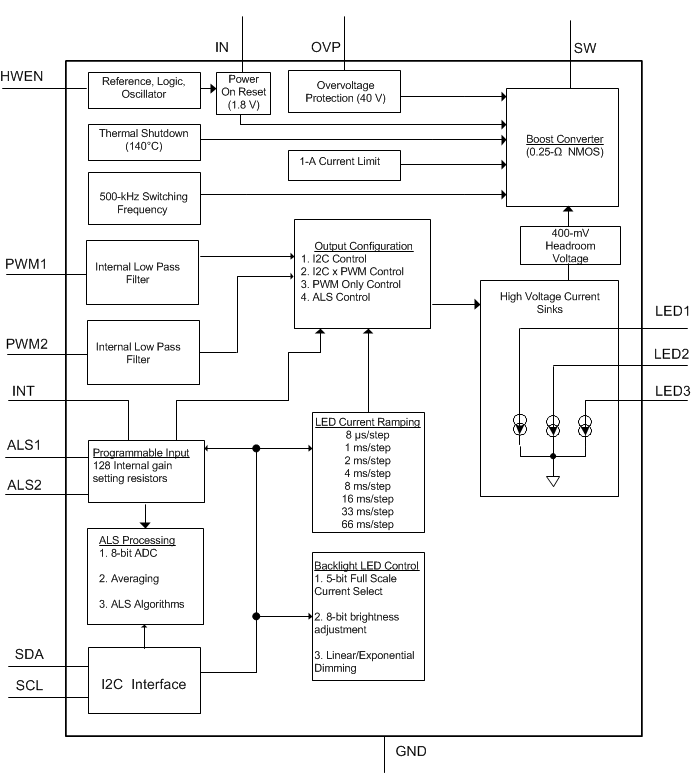
The LM3532 backlight driver consists of three 30-mA current sinks, a dual input ambient light sensor interface, and a dual input PWM control. The LED current can be controlled via either the I2C bus, the PWM input, the ambient light sensor interface, or a combination of each. The programmable options via I2C allow for the three current sinks to be controlled independently or be controlled by a single source.
7.2 Functional Block Diagram
7.3 Feature Description
7.3.1 40-V Boost Converter
The LM3532 contains a 40-V maximum output voltage, asynchronous boost converter with an integrated 250-mΩ switch, and three low-side current sinks. Each low-side current sink is independently programmable from 0 to 30 mA.
7.3.2 Hardware Enable Input
HWEN is the LM3532 device's global hardware enable input. This pin must be driven high to enable the device. HWEN is a high-impedance input so cannot be left floating. Typically HWEN would be connected through a pullup resistor to the logic supply voltage or driven high from a microcontroller. Driving HWEN low places the LM3532 into a low-current shutdown state and force all the internal registers to their power-on reset (POR) states.
7.3.3 Feedback Enable
Each current sink can be set for feedback enable or feedback disable. When feedback is enabled, the boost converter maintains at least 400 mV across each active current sink. This causes the boost output voltage (VOUT) to raise up or down depending on how many LEDs are placed in series in the highest voltage string. This ensures there is a minimum headroom voltage across each current sink. The potential drawback is that for large differentials in LED counts between strings, the LED voltage can be drastically different causing the excess voltage in the lower LED string to be dropped across its current sink. In situations where there are other voltage sources available, or where the LED count is low enough to use VIN as the power source, the feedback can be disabled on the specific current sink. This allows for the current sink to be active, but eliminates its control over the boost output voltage (see Figure 10). In this situation care must be taken to ensure there is always at least 400 mV of headroom voltage across each active current sink to avoid the current from going out of regulation. Control over the feedback enable/disable is programmable via the Feedback Enable Register (see Table 13).
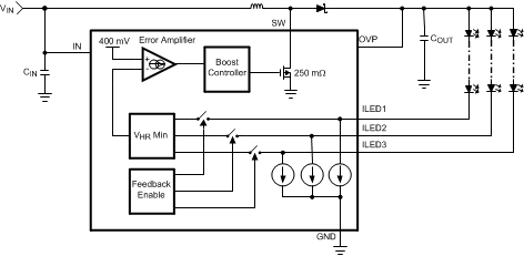 Figure 10. LM3532 Feedback Enable/Disable
7.3.4 LM3532 Current Sink Configuration
Control of the LM3532 device’s three current sinks is done by configuring the three internal control banks (Control A, Control B, and Control C) (see Figure 11). Any of the current sinks (ILED1, ILED2, or ILED3) can be mapped to any of the three control banks. Configuration of the control banks is done via the Output Configuration register.
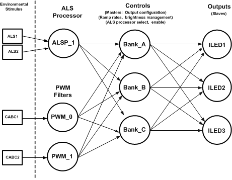 Figure 11. LM3532 Functional Control Diagram
7.3.5 PWM Inputs
The LM3532 provides two PWM inputs (PWM1 and PWM2) which can be mapped to any of the three Control Banks. PWM input mapping is done through the Control A PWM Configuration register, the Control B PWM Configuration register, and the Control C PWM Configuration register.
Both PWM inputs (PWM1 and PWM2) feed into internal level shifters and lowpass filters. This allows the PWM inputs to accept logic level signals and convert them to analog control signals which can control the assigned Control Banks LED current. The internal lowpass filter at each PWM input has a typical corner frequency of 540 Hz with a Q of 0.5. This gives a low end useful PWM frequency of around 2 kHz. Frequencies lower than this cause the LED current to show larger ripple and result in non-linear behavior vs. duty cycle due to the response time of the boost circuit. The upper boundary of the PWM frequency is greater than 100 kHz. Frequencies above 200 kHz begin to show non linear behavior due to propagation delays through the PWM input circuitry.
7.3.6 Full-Scale LED Current
There are 32 programmable full-scale current settings for each of the three control banks (Control A, Control B, and Control C). Each control bank has its own independent full-scale current setting (ILED_FULL_SCALE). Full-scale current for the respective Control Bank is set via the Control A Full-Scale Current Register, the Control B Full-Scale Current Register, and the Control C Full-Scale Current Register (see Table 12).
7.3.7 Interrupt Output
INT is an open drain output that pulls low when the ALS is enabled and when one of the ALS inputs transitions into a new zone. At the same time, the ALS Zone Information register is updated with the current ALS zone, and the software flag (bit 3 of the ALS Zone Information register) is written high. A readback of the Zone Information Register clears the software interrupt flag and reset the INT output to the open drain state. The active pulldown at INT is typically 125 Ω.
7.3.8 Protection Features
7.3.8.1 Overvoltage Protection
The LM3532 devices’s boost converter provides open-load protection, by monitoring the OVP pin. The OVP pin is designed to connect as close as possible to the positive terminal of the output capacitor. In the event of a disconnected load (LED current string with feedback enabled), the output voltage rises in order to try and maintain the correct headroom across the feedback enabled current sinks (see Table 13). Once VOUT climbs to the OVP threshold (VOVP) the boost converter is turned off, and switching stops until VOUT falls below the OVP hysteresis (VOVP – 1 V). Once the OVP hysteresis is crossed the LM3532 device’s boost converter begins switching again. In open load conditions this would result in a pulsed on/off operation.
7.3.8.2 Current Limit
The LM3532 device’s peak current limit in the NFET is set at typically 1 A (880 mA, minimum). During the positive portion of the switching cycle, if the NFET's current rises up to the current limit threshold, the NFET turns off for the rest of the switching cycle. At the start of the next switching cycle the NFET turns on again. For loads that cause the LM3532 to hit current limit each switching cycle, the output power can become clamped because the headroom across the feedback enabled current sinks is no longer being regulated when the device is in current limit. See Maximum Output Power below for guidelines on how peak current affects the LM3532 device's maximum output power.
7.4 Device Functional Modes
7.4.1 LED Current Ramping
The LM3532 provides 4 methods to control the rate of rise or fall of the LED current during these events:
- Start-up from 0 to the initial target
- Shutdown
- Ramp up from one brightness level to the next
- Ramp down from one brightness level to the next
7.4.2 Start-up and Shutdown Current Ramping
The start-up and shutdown ramp rates are independently programmable in the Start-up/Shutdown Ramp Rate register (see Table 4). There are 8 different start-up and 8 different shutdown ramp rates. The start-up ramp rates are independently programmable from the shutdown ramp rates, but not independently programmable for each Control Bank. For example, programming a start-up or shutdown ramp rate, programs the same ramp rate for each Control Bank.
7.4.3 Run-Time Ramp Rates
Current ramping from one brightness level to the next is programmed via the Run-Time Ramp Rate Register (see Table 5). There are 8 different ramp-up and 8 different ramp-down rates. The ramp-up rate is independently programmable from the ramp-down rate, but not independently programmable for each Control Bank. For example, programming a ramp-up or a ramp-down rate programs the same rate for each Control Bank.
7.4.4 LED Current Mapping Modes
All LED current brightness codes are 8 bits (256 different levels), where each bit represents a percentage of the programmed full-scale current setting for that particular Control Bank. The percentage of the full-scale current is different depending on which mapping mode is selected. The mapping mode can be either exponential or linear. Mapping mode is selected via bit [1] of the Control A, B, or C Brightness Configuration Registers.
7.4.5 Exponential Current Mapping Mode
In exponential mapping mode, the backlight code to LED current approximates the following equation:

where
- Code is the 8-bit code in the programmed brightness register
- DPWM is the duty cycle of the PWM input that is assigned to the particular control bank
Figure 12 shows the typical response of percentage of full-scale current setting vs 8-bit brightness code.
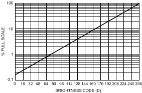 Figure 12. Exponential Mapping Response
7.4.6 Linear Current Mapping
In linear mapping mode the backlight code to LED current approximates Equation 2:

where
- Code is the 8-bit code in the programmed brightness register
- DPWM is the duty cycle of the PWM input that is assigned to the particular control bank.
For the linear mapped mode (Figure 13) shows the typical response of percentage of full-scale current setting vs 8-bit brightness code.
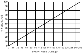 Figure 13. Linear Mapping Response
7.4.7 LED Current Control
Once the full-scale current is set, control of the LM3532 device’s LED current can be done via 2 methods:
- I2C Current Control
- Ambient Light Sensor Current Control
I2C current control allows for the direct control of the LED current by writing directly to the specific brightness register. In ambient light sensor current control the LED current is automatically set by the ambient light sensor interface.
7.4.7.1 I2C Current Control
I2C current control is accomplished by using one of the Zone Target Registers (for the respective Control Bank) as the brightness register. This is done via bits[4:2] of the Control (A, B, or C) Brightness Registers (see Table 9, Table 10, and Table 11). For example, programming bits[4:2] of the Control A Brightness Register with (000) makes the brightness register for Bank A (in I2C Current Control) the Control A Zone Target 0 Register.
7.4.7.2 I2C Current Control With PWM
I2C current control can also incorporate the PWM duty cycle at one of the PWM inputs (PWM1 or PWM2). In this situation the LED current is then a function of both the code in the programmed brightness register and the duty cycle input into the assigned PWM inputs (PWM1 or PWM2).
7.4.8 Assigning and Enabling a PWM Input
To make the backlight current a function of the PWM input duty cycle, one of the PWM inputs must first be assigned to a particular Control Bank. This is done via bit [0] of the Control A, B, or C PWM Registers (see Table 6, Table 7, or Table 8). After assigning a PWM input to a Control Bank, the PWM input is then enabled via bits [6:2] of the Control A/B/C PWM Enable Registers. Each enable bit is associated with a specific Zone Target Register in I2C Current Control. For example, if Control A Zone Target 0 Register is configured as the brightness register, then to enable PWM for that brightness register, Control A PWM bit [2] would be set to 1.
7.4.9 Enabling a Current Sink
Once the brightness register and PWM inputs are configured in I2C Current Control, the current sinks assigned to the specific control bank are enabled via the Control Enable Register (see Table 14). Table 1 below shows the possible configurations for Control Bank A in I2C Current Control. Table 1 would also apply to Control Bank B and Control Bank C.
Table 1. I2C Current Control and PWM Bit Settings (For Control Bank A)
| CURRENT SINK ASSIGNMENT | BRIGHTNESS REGISTER | PWM SELECT | PWM ENABLE | CURRENT SINK ENABLE |
|---|---|---|---|---|
| Output Configuration Register
Bits[1:0] = 00, assigns ILED1 to Control Bank A Bits[3:2] = 00 assigns ILED2 to Control Bank A Bits[5:4] = 00, assigns ILED3 to Control Bank A |
Control A Brightness Configuration Register Bits [4:2]
000 selects Control A Zone Target 0 as brightness register 001 selects Control A Zone Target 1 brightness register 010 selects Control A Zone Target 2 brightness register 011 selects Control A Zone Target 3 brightness register 1XX selects Control A Zone Target 4 brightness register |
Control A PWM Register Bit[0]
0 selects PWM1 1 selects PWM2 |
Control A PWM Register
Bit[2] is PWM enable when Control A Zone Target 0 is configured as the brightness register Bit[3] is PWM enable when Control A Zone Target 1 is configured as the brightness register Bit[4] is PWM enable when Control A Zone Target 2 is configured as the brightness register Bit[5] is PWM enable when Control A Zone Target 3 is configured as the brightness register Bit[6] is PWM enable when Control A Zone Target 4 is configured as the brightness register |
Control Enable Register Bit [0]
0 = Bank A Disabled 1 = Bank A Enabled |
7.4.10 Ambient Light Sensor Current Control
In Ambient Light Sensor (ALS) current control the LM3532 device’s backlight current is automatically set based upon the voltage at the ambient light sensor inputs (ALS1 and/or ALS2). These inputs are designed to connect to the outputs of analog ambient light sensors. Each ALS input has an active input voltage range of 0 to 2 V.
7.4.10.1 ALS Resistors
The LM3532 offers 32 separate programmable internal resistors at the ALS1 and ALS2 inputs. These resistors take the ambient light sensor's output current and convert it into a voltage. The value of the resistor selected is typically chosen such that the ambient light sensors output voltage swing goes from 0 to 2 V across the intended measured ambient light (LUX) range. The ALS resistor values are programmed via the ALS1 and ALS2 Resistor select registers (see Table 15). The code-to-resistor selection (assuming a 2-V full-scale voltage range) is shown in Equation 3:

Each higher code in the specific ALS Resistor Select Register increases the allowed ALS sensor current by 54 µA ( for a 2-V full-scale). When the ALS is disabled (ALS Configuration Register bit [3] = 0) the ALS inputs are set to a high impedance mode no matter what the ALS resistor selection is. Alternatively, ALS Resistor Select Register Code 00000 sets the specific ALS input to high impedance.
7.4.10.2 Ambient Light Zone Boundaries
The LM3532 provides 5 ambient light brightness zones which are defined by 4 zone boundary registers. The LM3532 has one set of zone boundary registers that is shared globally by all control banks. As the voltage at the ALS input changes in response to the ambient light sensors received light, the ALS voltage transitions through the 5 defined brightness zones. Each brightness zone can be assigned a brightness target via the 5 zone target registers. Each control bank has its own set of zone target registers. Therefore, in response to changes in a Brightness Zone at the ALS input, the LED current can transition to a new brightness level. This allows for backlit LCD displays to reduce the LED Current when the ambient light is dim or increase the LED current when the ambient light increases. Each zone boundary register is 8 bits with a full-scale voltage of 2 V. This gives 2 V/255 = 7.8 mV per bit. Figure 14 describes the ambient light to brightness mapping.
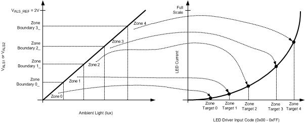 Figure 14. Ambient Light Input to Backlight Mapping
7.4.10.3 Ambient Light Zone Hysteresis
For each Zone Boundary there are two Zone Boundary Registers: a Zone Boundary High Register and a Zone Boundary Low Register. The difference between the Zone Boundary High and Zone Boundary Low Register set points (for a specific zone) creates the hysteresis that is required to transition between two adjacent zones. This hysteresis prevents the backlight current from oscillating between zones when the ALS voltage is close to a Zone Boundary Threshold. Figure 15 describes this Zone Boundary Hysteresis. The arrows indicate the direction of the ALS input voltage. The black dots indicate the threshold used when transitioning to a new zone.
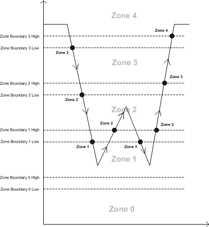 Figure 15. ALS Zone Boundaries + Hysteresis
7.4.10.4 PWM Enabled for a Particular Zone
The active PWM input for a specified control bank can be enabled/disabled for each ALS Brightness Zone. This is done via bits[6:2] of the corresponding Control A, B, or C PWM Registers (see Table 6, Table 7, and Table 8). For example, assuming Control Bank A is being used, then to make the PWM input active in Zones 0, 2, and 4, but not active in Zones 1, and 3; bits[6:2] of the Control A PWM Register would be set to (1, 0, 1, 0, 1).
7.4.10.5 ALS Operation
Figure 16 shows a functional block diagram of the LM3532's ambient light sensor interface.
 Figure 16. ALS Functional Block Diagram
7.4.10.6 ALS Input Select and ALS ADC Input
The internal 8-bit ADC digitizes the active ambient light sensor inputs (ALS1 or ALS2). The active ALS input is determined by the bit settings of the ALS input select bits, bits [7:6] in the ALS Configuration register. The active ALS input can be the average of ALS1 and ALS2, the maximum of ALS1 and ALS2, ALS1 only, or ALS2 only. Once the ALS input select stage selects the active ALS input, the result is sent to the internal 8-bit ADC. For example, if the active ALS input select is set to be the average of ALS1 and ALS2, then the voltage at ALS1 and ALS2 is first averaged, then applied to the ADC. The output of the ADC (ADC Register) is the digitized average value of ALS1 and ALS2.
The LM3532 device's internal ADC samples at 7.143 ksps. ADC timing is shown in Figure 17. When the ALS is enabled (ALS Configuration Register bit [3] = 1) the ADC begins sampling and converting the active ALS input. Each conversion takes 140 µs. After each conversion the ADC register is updated with new data.
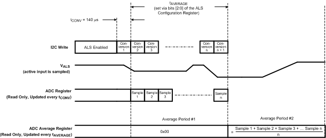 Figure 17. ADC Timing
7.4.10.7 ALS ADC Readback
The digitized value of the LM3532 device's ADC is read back from the ADC Readback Register. Once the ALS is enabled, the ADC begins converting the active ALS input and updating the ALS Readback Register every 140 µs. The ADC Readback register contains the updated data after each conversion.
7.4.10.8 ALS Averaging
ALS averaging is used to filter out any fast changes in the ambient light sensor inputs. This prevents the backlight current from constantly changing due to rapid fluctuations in the ambient light. There are 8 separate averaging periods available for the ALS inputs (see Table 17). During an average period the ADC continually samples at 7.143 ksps. Therefore, during an average period, the ALS Averager output is the average of 7143/tAVE.
7.4.10.9 ALS ADC Average Readback
The output of the LM3532's averager is read back via the Average ADC Register. This data is the ADC register data, averaged over the programmed ALS average time.
7.4.10.10 Initializing the ALS
On initial start-up of the ALS Block, the Ambient Light Zone defaults to Zone 0. This allows the ALS to start off in a predictable state. The drawback is that Zone 0 is often not representative of the true ALS Brightness Zone because the ALS inputs can get to their ambient light representative voltage much faster then the backlight is allowed to change. In order to avoid a multiple average time wait for the backlight current to get to its correct state, the LM3532 switches over to a fast average period (1.1 ms) on ALS startup. This quickly brings the ALS Brightness Zone (and the backlight current) to its correct setting (see Figure 18).
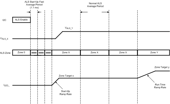 Figure 18. ALS Start-up Sequence
7.4.10.11 ALS Operation
The LM3532's Ambient Light Sensor Interface has 3 different algorithms that can be used to control the ambient light to backlight current response.
- Direct ALS Control
- Down Delay
ALS Algorithms
For each algorithm, the ALS follows these basic rules:
- For the ALS Interface to force a change in the backlight current (to a higher zone target), the averager output must have shown an increase for 3 consecutive average periods, or an increase and a remain at the new zone for 3 consecutive average periods.
- For the ALS Interface to force a change in the backlight current (to a lower zone target), the averager output must have shown a decrease for 3 consecutive average periods, or a decrease and remain at the new zone for 3 consecutive average periods.
- If condition 1 or condition 2 is satisfied, and during the next average period, the averager output changes again in the same direction as the last change, the LED current immediately changes at the beginning of the next average period.
- If condition 1 or condition 2 is satisfied and the next average period shows no change in the average zone, or shows a change in the opposite direction, then the criteria in step 1 or step 2 must be satisfied again before the ALS interface can force a change in the backlight current.
- The Averager Output (see Figure 16) contains the zone that is determined from the most recent full average period.
- The ALS Interface only forces a change in the backlight current at the beginning of an average period.
- When the ALS forces a change in the backlight current the change is to the brightness target pointed to by the zone in the Averager Output.
ALS Rules
7.4.10.12 Direct ALS Control
In direct ALS control the LM3532’s ALS Interface can force the backlight current to either a higher zone target or a lower zone target using the rules described in the ALS Rules Section.
Figure 19 shows the ALS voltage, the current average zone which is the zone determined by averaging the ALS voltage in the current average period, the Averager Output which is the zone determined from the previous full average period, and the target backlight current that is controlled by the ALS Interface. The following steps detail the Direct ALS algorithm:
- When the ALS is enabled the ALS fast start-up (1.1ms average period) quickly brings the Averager Output to the correct zone. This takes 3 fast average periods or approximately 3.3 ms.
- The 1st average period the ALS voltage averages to Zone 4.
- The 2nd average period the ALS voltage averages to Zone 3.
- The 3rd average period the ALS voltage averages to Zone 3 and the Averager Output shows a change from Zone 4 to Zone 3.
- The 4th average period the ALS voltage averages to Zone 2 and the Averager Output remains at its changed state of Zone 3.
- The 5th average period the ALS voltage averages to Zone 1. The Averager Output shows a change from Zone 3 to Zone 2. Because this is the 3rd average period that the Averager Output has shown a change in the decreasing direction from the initial Zone 4, the backlight current is forced to change to the current Averager Output (Zone 2's) target current.
- The 6th average period the ALS voltage averages to Zone 2. The Averager Output changes from Zone 2 to Zone 1. Because this is in the same direction as the previous change, the backlight current is forced to change to the current Averager Output (Zone 1's) target current.
- The 7th average period the ALS voltage averages to Zone 3. The Averager Output changes from Zone 1 to Zone 2. Because this change is in the opposite direction from the previous change, the backlight current remains at Zone 1's target.
- The 8th average period the ALS voltage averages to Zone 3. The Averager Output changes from Zone 2 to Zone 3.
- The 9th average period the ALS voltage averages to Zone 3. The Averager Output remains at Zone 3. Because this is the 3rd average period that the Averager Output has shown a change in the increasing direction from the initial Zone 1, the backlight current is forced to change to the current Averager Output (Zone 3's) target current.
- The 10th average period the ALS voltage averages to Zone 4. The Averager Output remains at Zone 3.
- The 11th average period the ALS voltage averages to Zone 4. The Averager Output changes to Zone 4.
- The 12th average period the ALS voltage averages to Zone 4. The Averager Output remains at Zone 4.
- The 13th average period the ALS voltage averages to Zone 4. The Averager Output remains at Zone 4. Because this is the 3rd average period that the Averager Output has shown a change in the increasing direction from the initial Zone 3, the backlight current is forced to change to the current Averager Output (Zone 4's) target current.
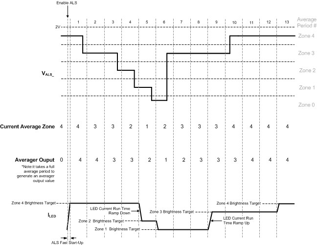 Figure 19. Direct ALS Control
7.4.11 Down Delay
The down-delay algorithm uses all the same rules from the ALS Rules section, except it provides for adding additional average period delays required for decreasing transitions of the Averager Output, before the LED current is programmed to a lower zone target current. The additional average period delays are programmed via the ALS Down-Delay register. The register provides 32 settings for increasing the down delay from 3 extra (code 00000) up to 34 extra (code 11111). For example, if the down-delay algorithm is enabled, and the ALS Down-Delay register were programmed with 0x00 (3 extra delays), then the Averager Output would need to see 6 consecutive changes in decreasing Zones (or 6 consecutive average periods that changed and remained lower), before the backlight current was programmed to the lower zones target current. Referring to Figure 20, assume that Down Delay is enabled and the ALS Down-Delay register is programmed with 0x02 (5 extra delays, 8 average period total delay for downward changes in the backlight target current):
- When the ALS is enabled the ALS fast start-up (1.1 ms average period) quickly brings the Averager Output to the correct zone. This takes 3 fast average periods or approximately 3.3 ms.
- The first average period the ALS averages to Zone 3.
- The second average period the ALS averages to Zone 2. The Averager Output remains at Zone 3.
- The 3rd through 7th average period the ALS input averages to Zone 2, and the Averager Output stays at Zone 2.
- The 8th average period the ALS input averages to Zone 4. The Averager Output remains at Zone 2.
- The 9th and 10th average periods the ALS input averages to Zone 4. The Averager Output is at Zone 4. Because the Averager Output increased from Zone 2 to Zone 4 and the required Down Delay time was not met (8 average periods), the backlight current was never changed to the Zone 2's target current.
- The 11th average period the ALS input averages to Zone 2. The Averager Output remains at Zone 4. Because this is the 3rd consecutive average period where the Averager Output has shown a change since the change from Zone 2, the backlight current transitions to Zone 4's target current.
- The 12th through 26th average periods the ALS input averages to Zone 2. The Averager Output remains at Zone 2. At the start of average period 20 the Down Delay algorithm has shown the required 8 average period delay from the initial change from Zone 4 to Zone 2. As a result the backlight current is programmed to Zone 2's target current.
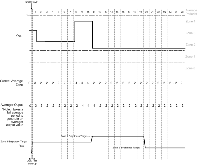 Figure 20. ALS Down-Delay Control
7.5 Programming
7.5.1 I2C-Compatible Interface
7.5.1.1 Start and Stop Conditions
The LM3532 is controlled via an I2C-compatible interface. START and STOP conditions classify the beginning and the end of the I2C session. A START condition is defined as SDA transitioning from HIGH-to-LOW while SCL is HIGH. A STOP condition is defined as SDA transitioning from LOW-to-HIGH while SCL is HIGH. The I2C master always generates the START and STOP conditions. The I2C bus is considered busy after a START condition and free after a STOP condition. During data transmission, the I2C master can generate repeated START conditions. A START and a repeated START conditions are equivalent function-wise. The data on SDA must be stable during the HIGH period of the clock signal (SCL). In other words, the state of SDA can only be changed when SCL is LOW.
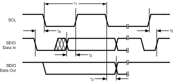 Figure 21. Start And Stop Sequences
7.5.1.2 I2C-Compatible Address
The 7-bit chip address for the LM3532 is (0x38) . After the START condition, the I2C master sends the 7-bit chip address followed by an eighth bit (LSB) read or write (R/W). R/W = 0 indicates a WRITE and R/W = 1 indicates a READ. The second byte following the chip address selects the register address to which the data is written. The third byte contains the data for the selected register.
 Figure 22. I2C-Compatible Chip Address (0x38)
7.5.1.3 Transferring Data
Every byte on the SDA line must be eight bits long, with the most significant bit (MSB) transferred first. Each byte of data must be followed by an acknowledge bit (ACK). The acknowledge related clock pulse (9th clock pulse) is generated by the master. The master then releases SDA (HIGH) during the 9th clock pulse. The LM3532 pulls down SDA during the 9th clock pulse, signifying an acknowledge. An acknowledge is generated after each byte has been received.
7.6 Register Maps
Table 2. LM3532 Register Descriptions
| NAME | ADDRESS | POWER-ON RESET |
|---|---|---|
| I2C Address | 0x38 (7 bit), 0x70 for Write and 0x71 for Read | |
| Output Configuration | 0x10 | 0xE4 |
| Startup/Shutdown Ramp Rate | 0x11 | 0xC0 |
| Run Time Ramp Rate | 0x12 | 0xC0 |
| Control A PWM | 0x13 | 0x82 |
| Control B PWM | 0x14 | 0x82 |
| Control C PWM | 0x15 | 0x82 |
| Control A Brightness | 0x16 | 0xF1 |
| Control A Full-Scale Current | 0x17 | 0xF3 |
| Control B Brightness | 0x18 | 0xF1 |
| Control B Full-Scale Current | 0x19 | 0xF3 |
| Control C Brightness | 0x1A | 0xF1 |
| Control C Full-Scale Current | 0x1B | 0xF3 |
| Feedback Enable | 0x1C | 0xFF |
| Control Enable | 0x1D | 0xF8 |
| ALS1 Resistor Select | 0x20 | 0xE0 |
| ALS2 Resistor Select | 0x21 | 0xE0 |
| ALS Down Delay | 0x22 | 0xE0 |
| ALS Configuration | 0x23 | 0x44 |
| ALS Zone Information | 0x24 | 0xF0 |
| ALS Brightness Zone | 0x25 | 0xF8 |
| ADC | 0x27 | 0x00 |
| ADC Average | 0x28 | 0x00 |
| ALS Zone Boundary 0 High | 0x60 | 0x35 |
| ALS Zone Boundary 0 Low | 0x61 | 0x33 |
| ALS Zone Boundary 1 High | 0x62 | 0x6A |
| ALS Zone Boundary 1 Low | 0x63 | 0x66 |
| ALS Zone Boundary 2 High | 0x64 | 0xA1 |
| ALS Zone Boundary 2 Low | 0x65 | 0x99 |
| ALS Zone Boundary 3 High | 0x66 | 0xDC |
| ALS Zone Boundary 3 Low | 0x67 | 0xCC |
| Control A Zone Target 0 | 0x70 | 0x33 |
| Control A Zone Target 1 | 0x71 | 0x66 |
| Control A Zone Target 2 | 0x72 | 0x99 |
| Control A Zone Target 3 | 0x73 | 0xCC |
| Control A Zone Target 4 | 0x74 | 0xFF |
| Control B Zone Target 0 | 0x75 | 0x33 |
| Control B Zone Target 1 | 0x76 | 0x66 |
| Control B Zone Target 2 | 0x77 | 0x99 |
| Control B Zone Target 3 | 0x78 | 0xCC |
| Control B Zone Target 4 | 0x79 | 0xFF |
| Control C Zone Target 0 | 0x7A | 0x33 |
| Control C Zone Target 1 | 0x7B | 0x66 |
| Control C Zone Target 2 | 0x7C | 0x99 |
| Control C Zone Target 3 | 0x7D | 0xCC |
| Control C Zone Target 4 | 0x7E | 0xFF |
7.6.1 Output Configuration
Table 3 configures how the three control banks are routed to the current sinks (ILED1, ILED2, ILED3)
Table 3. Output Configuration Register Description (Address 0x10)
7.6.2 Start-up/Shutdown Ramp Rate
This register controls the ramping of the LED current in current sinks ILED1, ILED2, and ILED3 during start-up and shutdown. The startup ramp rates/step are from when the device is enabled via I2C to when the target current is reached. The Shutdown ramp rates/step are from when the device is shut down via I2C until the LED current is 0. To start up and shut down the current sinks via I2C (see Equation 6).
Table 4. Start-up/Shutdown Ramp Rate Register Description (Address 0x11)
| Bits [7:6] | Bits [5:3] Shutdown Ramp |
Bits [2:0] Startup Ramp |
|---|---|---|
| Not Used | 000 = 8µs/step (2.048ms from Full-Scale to 0) (default)
001 = 1.024 ms/step (261 ms) 010 = 2.048 ms/step (522 ms) 011 = 4.096 ms/step (1.044s) 100 = 8.192 ms/step (2.088s) 101 = 16.384 ms/step (4.178s) 110 = 32.768 ms/step (8.356s) 111 = 65.536 ms/step (16.711s) |
000 = 8µs/step (2.048ms from Full-Scale to 0) (default)
001 = 1.024 ms/step (261ms) 010 = 2.048 ms/step (522ms) 011 = 4.096 ms/step (1.044s) 100 = 8.192 ms/step (2.088s) 101 = 16.384 ms/step (4.178s) 110 = 32.768 ms/step (8.356s) 111 = 65.536 ms/step (16.711s) |
7.6.3 Run-Time Ramp Rate
This register controls the ramping of the current in current sinks ILED1, ILED2, and ILED3. The Run Time ramp rates/step are from one current set-point to another after the device has reached its initial target set point from turn-on.
Table 5. Run Time Ramp Rate Register Description (Address 0x12)
| Bits [7:6] | Bits [5:3] Ramp Down |
Bits [2:0] Ramp Up |
|---|---|---|
| Not Used | 000 = 8µs/step (default)
001 = 1.024 ms/step 010 = 2.048 ms/step 011 = 4.096 ms/step 100 = 8.192 ms/step 101 = 16.384 ms/step 110 = 32.768 ms/step 111 = 65.536 ms/step |
000 = 8µs/step (default)
001 = 1.024 ms/step 010 = 2.048 ms/step 011 = 4.096 ms/step 100 = 8.192 ms/step 101 = 16.384 ms/step 110 = 32.768 ms/step 111 = 65.536 ms/step |
7.6.4 Control A PWM
This register configures which PWM input (PWM1 or PWM2) is mapped to Control Bank A and which zones the selected PWM input is active in.
Table 6. Control A Pwm Register Description (Address 0x13)
| Bit 7 N/A |
Bit 6 Zone 4 PWM Enable |
Bit 5 Zone 3 PWM Enable |
Bit 2 Zone 2 PWM Enable |
Bit 2 Zone 1 PWM Enable |
Bit 2 Zone 0 PWM Enable |
Bit 1 PWM Input Polarity |
Bit 0 PWM Select |
|---|---|---|---|---|---|---|---|
| Not Used | 0 = Active PWM input is disabled in Zone 4 (default) | 0 = Active PWM input is disabled in Zone 3 (default) | 0 = Active PWM input is disabled in Zone 2 (default) | 0 = Active PWM input is disabled in Zone 1 (default) | 0 = Active PWM input is disabled in Zone 0 (default) | 0 = active low polarity | 0 = PWM1 input is mapped to Control Bank A (default) |
| 1 = Active PWM input is enabled in Zone 4 | 1 = Active PWM input is enabled in Zone 3 | 1 = Active PWM input is enabled in Zone 2 | 1 = Active PWM input is enabled in Zone 1 | 1 = Active PWM input is enabled in Zone 0 | 1 = active high polarity (default) | 1 = PWM2 is mapped to Control Bank A |
7.6.5 Control B PWM
This register configures which PWM input (PWM1 or PWM2) is mapped to Control Bank B and which zones the selected PWM input is active in.
Table 7. Control B Pwm Register Description (Address 0x14)
| Bit 7 N/A |
Bit 6 Zone 4 PWM Enable |
Bit 5 Zone 3 PWM Enable |
Bit 2 Zone 2 PWM Enable |
Bit 2 Zone 1 PWM Enable |
Bit 2 Zone 0 PWM Enable |
Bit 1 PWM Input Polarity |
Bit 0 PWM Select |
|---|---|---|---|---|---|---|---|
| Not Used | 0 = Active PWM input is disabled in Zone 4 (default) | 0 = Active PWM input is disabled in Zone 3 (default) | 0 = Active PWM input is disabled in Zone 2 (default) | 0 = Active PWM input is disabled in Zone 1 (default) | 0 = Active PWM input is disabled in Zone 0 (default) | 0 = active low polarity | 0 = PWM1 input is mapped to Control Bank B (default) |
| 1 = Active PWM input is enabled in Zone 4 | 1 = Active PWM input is enabled in Zone 3 | 1 = Active PWM input is enabled in Zone 2 | 1 = Active PWM input is enabled in Zone 1 | 1 = Active PWM input is enabled in Zone 0 | 1 = active high polarity (default) | 1 = PWM2 is mapped to Control Bank B |
7.6.6 Control C PWM
This register configures which PWM input (PWM1 or PWM2) is mapped to Control Bank C and which zones the selected PWM input is active in.
Table 8. Control C Pwm Register Description (Address 0x15)
| Bit 7 N/A |
Bit 6 Zone 4 PWM Enable |
Bit 5 Zone 3 PWM Enable |
Bit 2 Zone 2 PWM Enable |
Bit 2 Zone 1 PWM Enable |
Bit 2 Zone 0 PWM Enable |
Bit 1 PWM Input Polarity |
Bit 0 PWM Select |
|---|---|---|---|---|---|---|---|
| Not Used | 0 = Active PWM input is disabled in Zone 4 (default) | 0 = Active PWM input is disabled in Zone 3 (default) | 0 = Active PWM input is disabled in Zone 2 (default) | 0 = Active PWM input is disabled in Zone 1 (default) | 0 = Active PWM input is disabled in Zone 0 (default) | 0 = active low polarity | 0 = PWM1 input is mapped to Control Bank C (default) |
| 1 = Active PWM input is enabled in Zone 4 | 1 = Active PWM input is enabled in Zone 3 | 1 = Active PWM input is enabled in Zone 2 | 1 = Active PWM input is enabled in Zone 1 | 1 = Active PWM input is enabled in Zone 0 | 1 = active high polarity (default) | 1 = PWM2 is mapped to Control Bank C |
7.6.7 Control A Brightness Configuration
The Control A Brightness Configuration Register has 3 functions:
- Selects how the LED current sink which is mapped to Control Bank A is controlled (either directly through the I2C or via the ALS interface).
- Programs the LED current mapping mode for Control Bank A (Linear or Exponential).
- Programs which Control A Zone Target Register is the Brightness Register for Bank A in I2C Current Control.
Table 9. Control A Brightness Configuration Register Description (Address 0x16)
| Bits [7:5] Not Used |
Bits [4:2] Control A Brightness Pointer (I2C Current Control Only) |
Bit 1 LED Current Mapping Mode |
Bit 0 Bank A Current Control |
|---|---|---|---|
| N/A | 000 = Control A Zone Target 0 001 = Control A Zone Target 1 010 = Control A Zone Target 2 011 = Control A Zone Target 3 1XX = Control A Zone Target 4 (default) |
0 = Exponential Mapping (default)
1 = Linear Mapping |
0 = ALS Current Control 1 = I2C Current Control (default) |
7.6.8 Control B Brightness Configuration
The Control B Brightness Configuration Register has 3 functions:
- Selects how the LED current sink which is mapped to Control Bank B is controlled (either directly through the I2C or via the ALS interface).
- Programs the LED current mapping mode for Control Bank B (Linear or Exponential).
- Programs which Control B Zone Target Register is the Brightness Register for Bank B in I2C Current Control.
Table 10. Control B Brightness Configuration Register Description (Address 0x18)
| Bits [7:5] Not Used |
Bits [4:2] Control A Brightness Pointer (I2C Current Control Only) |
Bit 1 LED Current Mapping Mode |
Bit 0 Bank B Current Control |
|---|---|---|---|
| N/A | 000 = Control B Zone Target 0 001 = Control B Zone Target 1 010 = Control B Zone Target 2 011 = Control B Zone Target 3 1XX = Control B Zone Target 4 (default) |
0 = Exponential Mapping (default)
1 = Linear Mapping |
0 = ALS Current Control 1 = I2C Current Control (default) |
7.6.9 Control C Brightness Configuration
The Control C Brightness Configuration Register has 3 functions:
- Selects how the LED current sink which is mapped to Control Bank C is controlled (either directly through the I2C or via the ALS interface)
- Programs the LED current mapping mode for Control Bank C (Linear or Exponential)
- Programs which Control C Zone Target Register is the Brightness Register for Bank C in I2C Current Control
Table 11. Control C Brightness Configuration Register Description (Address 0x1a)
| Bits [7:5] Not Used |
Bits [4:2] Control C Brightness Pointer (I2C Current Control Only) |
Bit 1 LED Current Mapping Mode |
Bit 0 Bank C Current Control |
|---|---|---|---|
| N/A | 000 = Control C Zone Target 0 001 = Control C Zone Target 1 010 = Control C Zone Target 2 011 = Control C Zone Target 3 1XX = Control C Zone Target 4 (default) |
0 = Exponential Mapping (default)
1 = Linear Mapping |
0 = ALS Current Control 1 = I2C Current Control (default) |
7.6.10 Control A, B, and C Full-Scale Current
These registers program the full-scale current setting for the current sink(s) assigned to Control Bank A, B, and C. Each Control Bank has its own full-scale current setting (Control Bank A, Address 0x17), (Control Bank B, address 0x19), (Control Bank C, address 0x1B).
Table 12. Control A/B/C Full-Scale Current Registers Descriptions (Address 0x17, 0x19, 0x1b)
| Bits [7:5] Not Used |
Bits [4:0] Control A/B/C Full-Scale Current Select Bits |
|---|---|
| N/A | 00000 = 5 mA |
| 00001 = 5.8 mA | |
| 00010 = 6.6 mA | |
| 00011 = 7.4 mA | |
| 00100 = 8.2 mA | |
| 00101 = 9 mA | |
| 00110 = 9.8 mA | |
| 00111 = 10.6 mA | |
| 01000 = 11.4 mA | |
| 01001 = 12.2 mA | |
| 01010 = 13 mA | |
| 01011 = 13.8 mA | |
| 01100 = 14.6 mA | |
| 01101 = 15.4 mA | |
| 01110 = 16.2 mA | |
| 01111 = 17 mA | |
| 10000 = 17.8 mA | |
| 10001 = 18.6mA | |
| 10010 = 19.4 mA | |
| 10011 = 20.2 mA (default) | |
| 10100 = 21 mA | |
| 10101 = 21.8 mA | |
| 10110 = 22.6 mA | |
| 10111 = 23.4 mA | |
| 11000 = 24.2 mA | |
| 11001 = 25 mA | |
| 11010 = 25.8 mA | |
| 11011 = 26.6 mA | |
| 11100 = 27.4 mA | |
| 11101 = 28.2 mA | |
| 11110 = 29 mA | |
| 11111 = 29.8 mA |
7.6.11 Feedback Enable
The Feedback Enable Register configures which current sinks are or are not part of the boost control loop.
Table 13. Feedback Enable Register Description (Address 0x1c)
| Bits [7:3] Not Used |
Bit 2 ILED3 Feedback Enable |
Bit 1 ILED2 Feedback Enable |
Bit 0 ILED1 Feedback Enable |
||
|---|---|---|---|---|---|
| N/A | 0 = ILED3 is not part of the boost control loop 1 = ILED3 is part of the boost control loop (default) |
0 = ILED2 is not part of the boost control loop 1 = ILED2 is part of the boost control loop (default) |
0 = ILED1 is not part of the boost control loop 1 = ILED1 is part of the boost control loop (default) |
||
7.6.12 Control Enable
The Control Enable register contains the bits to turn on/off the individual Control Banks (A, B, or C). Once one of these bits is programmed high, the current sink(s) assigned to the selected control banks are enabled.
Table 14. Control Enable Register Description (Address 0x1d)
| Bits (7:3) (Not Used) |
Bit 2 Control C Enable |
Bit 1 Control B Enable |
Bit 0 Control A Enable |
||
|---|---|---|---|---|---|
| N/A | 0 = Control C is disabled (default)
1 = Control C is enabled |
0 = Control B is disabled (default)
1 = Control B is enabled |
0 = Control A is disabled (default)
1 = Control A is enabled |
||
7.6.13 ALS1 and ALS2 Resistor Select
The ALS Resistor Select Registers program the internal pulldown resistor at the ALS1/ALS2 input. Each ALS input has its own resistor select register (ALS1 Resistor Select Register, Address 0x20) and (ALS2 Resistor Select Register, Address 0x21). Each ALS input can be set independent of the other. There are 32 available resistors including a high impedance setting. The full-scale input voltage range at either ALS input is 2V.
Table 15. ALS Resistor Select Register Description (Address 0x20, Address 0x21)
| Bit [7:5] Not Used |
Bit [4:0] ALS1/ALS2 Resistor Select Bits |
|---|---|
| N/A | 00000 = High Impedance (default) |
| 00001 = 37 kΩ | |
| 00010 = 18.5 kΩ | |
| 00011 = 12.33 kΩ | |
| 00100 = 9.25 kΩ | |
| 00101 = 7.4 kΩ | |
| 00110 = 6.17 kΩ | |
| 00111 = 5.29 kΩ | |
| 01000 = 4.63 kΩ | |
| 01001 = 4.11 kΩ | |
| 01010 = 3.7 kΩ | |
| 01011 = 3.36 kΩ | |
| 01100 = 3.08 kΩ | |
| 01101 = 2.85 kΩ | |
| 01110 = 2.64 kΩ | |
| 01111 = 2.44 kΩ | |
| 10000 = 2.31 kΩ | |
| 10001 = 2.18 kΩ | |
| 10010 = 2.06 kΩ | |
| 10011 = 1.95 kΩ | |
| 10100 = 1.85 kΩ | |
| 10101 = 1.76 kΩ | |
| 10110 = 1.68 kΩ | |
| 10111 = 1.61 kΩ | |
| 11000 = 1.54 kΩ | |
| 11001 = 1.48 kΩ | |
| 11010 = 1.42 kΩ | |
| 11011 = 1.37 kΩ | |
| 11100 = 1.32 kΩ | |
| 11101 = 1.28 kΩ | |
| 11110 = 1.23 kΩ | |
| 11111 = 1.19 kΩ |
7.6.14 ALS Down Delay
The ALS Down-Delay Register adds additional average time delays for ALS changes in the backlight current during falling ALS input voltages. Code 00000 adds 3 extra average period delays on top of the 3 default delays (6 total). Code 11111 adds 34 extra average period delays.
Table 16. ALS Down Delay Register Description (Address 0x22)
| Bits [7:6] Not Used |
Bit [5] ALS Fast Start-up Enable |
Bits [4:0] Down Delay |
|---|---|---|
| N/A | 0 = ALS Fast start-up is Disabled 1 = ALS Fast start-up is Enabled (default) |
00000 = 6 total average period delay for down-delay control (default)
: : : 11111 = 34 total average periods of delay for down delay control |
7.6.15 ALS Configuration
The ALS Configuration register controls the ALS average times, the ALS enable bit, and the ALS input select.
Table 17. ALSConfiguration Register Description (Address 0x23)
| Bits [7:6] ALS Input Select |
Bit [5:4] ALS Control |
Bit 3 ALS Enable |
Bits [2:0] ALS Average Time |
|---|---|---|---|
| 00 = Average of ALS1 and ALS2 is used to determine backlight current 01 = Only the ALS1 input is used to determine backlight current (default) 10 = Only the ALS2 input is used to determine the backlight current 11 = The maximum of ALS1 and ALS2 is used to determine the backlight current |
00 = Direct ALS Control. ALS inputs respond to up and down transitions (default)
01 = This setting is for a future mode. 1X = Down Delay Control. Extra delays of 3 x tAVE to 34 x tAVE are added for down transitions, before the new backlight target is programmed. (see Down Delay section). |
0 = ALS is disabled (default)
1 = ALS is enabled |
000 = 17.92 ms 001 = 35.84 ms 010 = 71.68 ms 011 = 143.36 ms 100 = 286.72 ms (default) 101 = 573.44 ms 110 = 1146.88 ms 111 = 2293.76 ms |
7.6.16 ALS Zone Readback / Information
The ALS Zone Readback and ALS Zone Information Readback registers each contain information on the current ambient light brightness zone. The ALS Zone Readback register contains the ALS Zone after the averager and discriminator block and reflects both up and down changes in the ambient light brightness zone. The ALS Zone Information register reflects the contents of either the ALS Zone Readback register (with up and down transition). This register also includes a Zone Change bit (bit 3) which is written with a 1 each time the ALS zone changes. This bit is cleared upon read back of the ALS Zone Information register.
Table 18. ALS Zone Information Register Description (Address 0x24)
| Bits [7:4] Not Used |
Bit 3 Zone Change Bit |
Bits [2:0] Brightness Zone |
|---|---|---|
| N/A | 0 = No change in ALS Zone (default)
1 = There was a change in the ALS Zone since the last read of this register. This bit is cleared on read back. |
000 = Zone 0 (default)
001 = Zone 1 010 = Zone 2 011 = Zone 3 1XX = Zone 4 |
Table 19. ALS Zone Readback Register Description (Address 0x25)
| Bits [7:3] Not Used |
Bits [2:0] Brightness Zone |
|---|---|
| N/A | 000 = Zone 0 (default)
001 = Zone 1 010 = Zone 2 011 = Zone 3 1XX = Zone 4 |
7.6.17 ALS Zone Boundaries
There are 4 ALS Zone Boundary registers which form the boundaries for the 5 Ambient Light Zones. Each Zone Boundary register is 8 bits with a maximum voltage of 2V. This gives a step size for each Zone Boundary Register bit of:

| ALS Zone Boundary 0 High (Address 0x60), default = 0x35 (415.7 mV) |
| ALS Zone Boundary 0 Low (Address 0x61), default = 0x33 (400 mV) |
|
Line-Break |
| ALS Zone Boundary 1 High (Address 0x62), default = 0x6A (831.4 mV) |
| ALS Zone Boundary 1 Low (Address 0x63), default = 0x66 (800 mV) |
|
Line-Break |
| ALS Zone Boundary 2 High (Address 0x64), default = 0xA1 (1262.7 mV) |
| ALS Zone Boundary 2 Low (Address 0x65), default = 0x99 (1200 mV) |
|
Line-Break |
| ALS Zone Boundary 3 High (Address 0x66), default = 0xDC (1725.5 mV) |
| ALS Zone Boundary 3 Low (Address 0x67), default = 0xCC (1600 mV) |
7.6.18 Zone Target Registers
There are 3 groups of Zone Target Registers (Control A, Control B, and Control C). The Zone Target registers have 2 functions. In Ambient Light Current control, they map directly to the corresponding ALS Zone. When the active ALS input lands within the programmed Zone, the backlight current is programmed to the corresponding zone target registers set point (see below).
| Control A Zone Target Register 0 maps directly to Zone 0 (Address 0x70) |
| Control A Zone Target Register 1 maps directly to Zone 1 (Address 0x71) |
| Control A Zone Target Register 2 maps directly to Zone 2 (Address 0x72) |
| Control A Zone Target Register 3 maps directly to Zone 3 (Address 0x73) |
| Control A Zone Target Register 4 maps directly to Zone 4 (Address 0x74) |
| Line-Break |
| Control B Zone Target Register 0 maps directly to Zone 0 (Address 0x75) |
| Control B Zone Target Register 1 maps directly to Zone 1 (Address 0x76) |
| Control B Zone Target Register 2 maps directly to Zone 2 (Address 0x77) |
| Control B Zone Target Register 3 maps directly to Zone 3 (Address 0x78) |
| Control B Zone Target Register 4 maps directly to Zone 4 (Address 0x79) |
| Control C Zone Target Register 0 maps directly to Zone 0 (Address 0x7A) |
| Control C Zone Target Register 1 maps directly to Zone 1 (Address 0x7B) |
| Control C Zone Target Register 2 maps directly to Zone 2 (Address 0x7C) |
| Control C Zone Target Register 3 maps directly to Zone 3 (Address 0x7D) |
| Control C Zone Target Register 4 maps directly to Zone 4 (Address 0x7E) |
In I2C Current Control, any of the 5 Zone Target Registers for the particular Control Bank can be the LED brightness registers. This is set according to Control A, B, or C Brightness Configuration Registers (Bits [4:2]).