SNVS594G December 2008 – April 2016 LM3555
PRODUCTION DATA.
- 1 Features
- 2 Applications
- 3 Description
- 4 Revision History
- 5 Pin Configuration and Functions
- 6 Specifications
-
7 Detailed Description
- 7.1 Overview
- 7.2 Functional Block Diagram
- 7.3 Feature Description
- 7.4 Device Functional Modes
- 7.5 Programming
- 7.6 Register Maps
- 8 Application and Implementation
- 9 Power Supply Recommendations
- 10Layout
- 11Device and Documentation Support
- 12Mechanical, Packaging, and Orderable Information
Package Options
Mechanical Data (Package|Pins)
- YZR|12
Thermal pad, mechanical data (Package|Pins)
Orderable Information
7 Detailed Description
7.1 Overview
The LM3555 is a high-power white-LED flash driver capable of delivering up to 500 mA of LED current into a single LED, or up to 400 mA into two series LEDs. The device incorporates a 2-MHz constant frequency, synchronous, current mode PWM boost converter, and a single high-side current source to regulate the LED current over the 2.5 V to 5.5 V input voltage range. Dual control interfaces (simple ENABLE control or I2C) and diode detection (single LED or two LEDs in series) make the LM3555 highly adaptable to a large variety of designs.
7.2 Functional Block Diagram
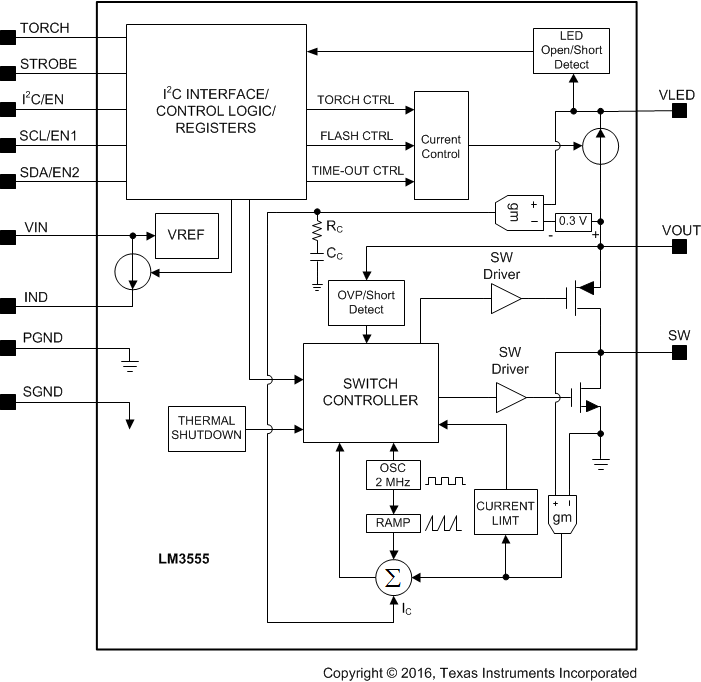
7.3 Feature Description
7.3.1 Synchronous Boost Converter
The LM3555 operates in two modes: LED boost mode or LED pass mode. When the input voltage is above the LED voltage plus current source headroom voltage the device turns the PFET on continuously (pass mode). In pass mode the difference between (VIN – ILED × RON_P) and the voltage across the LEDs is dropped across the current source. When the output voltage (VOUT) is greater than the input voltage (VIN) minus approximately 200 mV, the PWM converter switches and maintains at least 300 mV across the current source (LED boost mode). This minimum headroom voltage ensures that the current sinks remain in regulation.
Once the LM3555 transitions from pass mode to boost mode, the device does not return to pass mode until the device is disabled and re-enabled. At this point, the converter re-evaluates the conditions and enter the appropriate mode.
7.3.2 High-Side Current Source
The high-side current source of the LM3555 is capable of driving one or two LEDs in series. Depending on the configuration, the LM3555 automatically sets default diode current levels and diode current limits. For a single LED, the flash current range is 200 mA to 500 mA in 20-mA steps with a default current equal to 500 mA. For two LEDs in series, the flash current range is 200 mA to 400 mA in 20-mA steps with a default current equal to 320 mA.
Additionally, the high-side current source is capable of supporting assist/torch current levels (continuous current) between 60 mA and 160 mA in 20-mA levels.
7.3.3 I2C/EN Pin
The I2C/EN pin on the LM3555 changes the control interface depending on its state. To use the LM3555 in the simple control mode, the I2C/EN pin must be tied low. To use the LM3555 in I2C control mode, the I2C/EN pin must be tied high. Toggling this pin between simple control mode and I2C control mode is not recommended.
7.3.4 SDA/EN2 and SCL/EN1 Pins
Depending on the state of the I2C/EN pin, the SDA/EN2 and SCL/EN1 pins function in different ways. If the I2C/EN pin is equal to a 1, the SDA/EN2 pin functions as an I2C SDA (data) pin, and the SCL/EN1 pin functions as an I2C SCL (clock) pin. If the I2C/EN pin is equal to a 0, the SDA/EN2 pin functions as the simple control pin EN2, and the SCL/EN1 pin functions as the simple control pin EN1.
When using the simple control mode, the flash, torch, and indicator modes can be enabled. In simple control mode, internal pulldown resistors on the SDA/EN2 and SCL/EN1 pins become active. In I2C control mode, these pulldowns become disabled.
7.3.5 STROBE Pin
The STROBE pin of the LM3555 provides an external method for initiating a flash event. In most cases, the STROBE pin is connected to an imaging module so that the image capture and flash event are synchronized. The STROBE pin is only functional when the LM3555 is placed into I2C control mode (I2C/EN = 1) and the output on (OEN in 0x04) and strobe signal Mode (SEN in 0x04) bits are set (1). The STROBE pin can be configured to be an edge sensitive or level sensitive input by setting the strobe signal usage bit (SSU in 0x04. 1 = Level, 0 = Edge). In edge sensitive mode, a rising edge transition (0 to 1) starts the flash event, and the internal flash timer terminates the event. In level sensitive mode, a rising edge transition (0 to 1) starts the flash event and a falling edge transition (1 to 0) or the internal flash timer, whichever occurs first, terminates the event. In I2C mode, there is an internal pulldown resistor that becomes enabled on the STROBE pin.
In simple control mode, the STROBE pin functions as a output when a pullup resistor is connected, alerting the user to the number of flash LEDs present in the system. If the STROBE pin is outputting a 1, two LEDs are present, whereas a 0 indicates a single LED is present.
7.3.6 TORCH Pin
The TORCH pin of the LM3555, depending on the state and configuration, allows the user to enable torch/assist mode without having to write the command through the I2C bus or through toggling the EN1 and EN2 pins. In simple mode, the LM3555 drives 60 mA of LED current if two series LEDs are present and 80 mA is one LED is present. In I2C mode, the external torch mode bit (TEN in register 0x04) must be set to a 1 to allow an external torch (default value = 1). In I2C mode, the torch mode current is equal to the Assist mode current level stored in register 0x03. The TORCH pin has an internal pulldown resistor enabled in both simple mode and I2C mode.
7.3.7 Indicator LED Pin (IND)
The indicator LED current source pin (IND) is able to drive a single red indicator LED when the anode is connected to the LM3555 and the cathode is connected to ground. In simple logic mode, the default indicator current is 2.5 mA, and in I2C mode, the indicator LED current can be adjusted to 2.5 mA, 5 mA, 7.5 mA, or 10 mA.
7.3.8 Internal Diode Detection
During the start-up sequence of the LM3555 an internal voltage comparator on the VLED pin monitors the forward voltage of the LED or LEDs. This measurement occurs when the ramp-up current reaches 80 mA. If, at this time, the diode voltage exceeds the user-selectable diode detect threshold (Register 0x02 bits VO1 and VO0), the LM3555 assumes two series LEDs are present and limits the maximum flash current to 400 mA. The four adjustable levels are; 00 = 4.35 V, 01 = 4.65 V, 10 = 4.05 V and 11 = 4.95 V. This detection feature can be disabled by setting the diode detect enable bit (DEN) in the Current Set Register (address 0x03) to a 0. The DEN bit is set to a 1 (enabled) by default.
In all cases during start-up, the diode current first ramps to 80 mA and then proceeds to the target current. If the torch/assist current is set to 60 mA, the LM3555 first reaches 80 mA and then drop to 60 mA.
The number of LEDs present in the system is recorded in a read-only diode number (DN) bit of the fault register (address 0x05). In simple mode, the number of LEDs present are output on the STROBE pin (0 = 1 LED, 1 = 2 LEDs).
7.3.9 Fault Protections
The LM3555 has a number of fault protection mechanisms designed to not only protect the LM3555 device itself, but also the rest of the system. Active faults protections include:
- Overvoltage protection (VOUT)
- Short-Circuit protection (VOUT and VLED)
- Overtemperature protection
- Flash timeout
- Indicator LED protection (open and short)
- Broken inductor protection
In the event that any of these faults occur, the LM3555 sets a flag in the Fault Register (Address 0x05) and places the device into standby or shutdown. In simple control mode, normal operation cannot resume until the fault has been fixed and until EN1 and EN2 are driven low 0. In I2C control mode, normal operation cannot resume until the fault has be fixed and until an I2C read of the faults register (0x05) has completed. The act of reading the fault register clears the fault bits.
7.3.9.1 Output Overvoltage Protection (OVP)
An OVP fault is triggered when the output voltage of the LM3555 reaches a value greater than 9.5 V (typical). The OVP condition is cleared when the output voltage (VOUT) is able to operate below 9.5 V. An output capacitor or an LED that has become an open circuit can cause an OVP event to occur. This fault is reported to the OVP fault bit in the Fault Register (bit7 in address 0x05).
7.3.9.2 Output and LED Short-Circuit Protection (SCP)
An SCP fault is triggered when the output voltage (VOUT) and/or the VLED pin does not reach 0.8 V in 0.5 ms. The short circuit condition is cleared when the output (VOUT) is allowed to reach its steady state target and when the LED voltage rises above 0.8 V. A shorted output capacitor or a shorted LED could cause this fault to occur. This fault is reported to the SC fault bit in the Fault Register (bit6 in address 0x05).
7.3.9.3 Overtemperature Protection (OTP)
An OTP fault is triggered when the diode junction temperature of the LM3555 reaches an internal temperature of around 150°C. The OTP condition is cleared when the junction temperature falls below 140°C. A printed circuit board (PCB) with poor thermal dissipation properties and very high ambient temperatures (greater that 85°C) could cause this fault to occur. Refer to AN-1112 DSBGA Wafer Level Chip Scale Package (SNVA009) for more information regarding proper PCB layout. This fault is reported to the OTP fault bit in the Fault Register (bit5 in address 0x05).
7.3.9.4 Flash Timeout (FTP)
An FTP fault is triggered any time the flash pulse duration reaches the flash timeout duration. In I2C control mode, the FTP fault is triggered whenever a flash is initiated through the Control Register (OEN and OM1/OM0 bits) or through an edge-sensitive strobe event. A FTP fault could occur in simple control Mode if the controller tied to EN1 and EN2 pins cannot toggle the pins low at the desired pulse rate. This same condition could occur with a level-sensitive strobe event controlled by a camera module. This fault is reported to the TO fault bit in the Fault Register (bit4 in address 0x05). A FTP fault is the only reported fault that does not need to be cleared before any additional LED event can occur.
7.3.9.5 Indicator Fault (IF)
An IF fault is triggered when the voltage on the IND pin is greater than 2.571 V or less than 0.842 V. This fault indicates that there is either an open or a short present on the IND pin. The short-circuit condition is cleared when the IND pin is allowed to operate between 0.842 V and 2.571 V. A shorted or open indicator LED could cause this fault to occur. This fault is reported to the IF fault bit in the Fault Register (bit2 in address 0x05).
7.3.9.6 Broken Inductor Fault (IP)
An IP fault is triggered when the LM3555 detects that the inductance of the inductor has dropped below an acceptable value. This fault indicates that the inductor has been damaged. An inductor that has had its ferrite material damaged could cause this fault to occur. This fault is reported to the IP fault bit in the Fault Register (bit1 in address 0x05).
7.3.10 Undervoltage Lockout (UVLO)
The LM3555 has a UVLO feature that disables the operation of the device in the event that the input voltage falls below 2.4 V (typical). In simple control mode, the input voltage must increase to at least 2.47 V (typical), and the EN1 and EN2 pins must be toggled low (0) before normal operation can resume.
In I2C control mode, the output enable bit in the Control Register (Address 0x04) is set to a 0 in the event of a UVLO occurrence. The input voltage must rise to at least 2.47 V before the LM3555 becomes fully functional again.
A UVLO event does not disturb the state of the other registers of the LM3555.
7.3.11 Power-On Reset (POR)
A POR circuit is present on the LM3555 for use in I2C control mode. The POR circuit ensures that the device starts in a known OFF state and that the registers used in the I2C control interface are initialized to the proper start-up values once the input voltage reaches a voltage greater than 1.8 V (typical). An input voltage lower than 1.8 V not only places the device into UVLO, but also clears all of the LM3555 registers.
7.4 Device Functional Modes
7.4.1 Single LED Operation
In single LED operation, the LED flash current is allowed to reach the maximum level of 500 mA. By default, the assist/torch current is set to 80 mA, and the flash current is set to 500 mA.
For input voltages that are higher than the LED forward voltage, the LM3555 operates in a pass mode. As VIN drops, the LM3555 first transitions from pass mode to the minimum duty-cycle boost mode. In this mode, the output voltage (VOUT) increases to a level higher than needed to maintain current regulation through the current source. If VIN continues to decrease, the LM3555 transitions again, this time from minimum duty-cycle boost mode to standard boost mode. Standard boost mode adjusts the converters duty cycle to maintain 300 mV across the current source of the device.
Once the LM3555 transitions from pass mode to either boost mode, the device stays in one of those boost modes until the device is disabled or timed-out and then restarted.
7.4.2 Dual LED Operation
In dual LED operation, the LED flash current is allowed to reach a maximum level of 400 mA. By default, the assist/torch current is set to 60 mA, and the flash current is set to 320 mA.
During dual LED operation, the output voltage is always greater than the input voltage (assuming standard white flash LEDs are used), forcing the LM3555 to be in boost mode over the entire input voltage range.
7.4.3 Torch or Assist (Continuous Current) Operation
There are two different continuous current modes on the LM3555: torch and assist.
Torch mode is enabled through the use of the dedicated TORCH pin using both simple and I2C modes (1 = Torch, 0 = Standby (I2C mode) or shutdown (simple mode). In I2C control mode, the TORCH pin functionality can be enabled and disabled through by setting the value of the TEN bit in the Control Register (Address 0x04). TEN = 1 allows an external torch while TEN = 0 does not.
Assist mode is enabled in simple control mode by driving EN1 low (0) and by driving EN2 high (1). In I2C control mode, assist mode is enabled by setting the output mode bits (OM1 and OM0) to 10 and setting the output enable bit (OEN) to a 1 in the Control Register (0x04). Assist mode remains active in I2C mode until the OEM bit is set to 0 or until a flash event occurs.
The LM3555 can drive one or two LEDs at continuous current levels ranging from 60 mA to 160 mA in 20-mA steps. In simple control mode, the torch and assist current levels are equal to 60 mA for two LEDs or 80 mA for a single LED. In I2C mode, the current is set in the Current Set Register (Address 0x30, AC2-AC0 bits).
7.4.4 Flash (Pulsed Current) Operation
A flash event using the LM3555 can be initiated though the dedicated control interface in both simple and I2C modes, and through the use of the STROBE pin in I2C mode.
By driving both EN1 and EN2 high (1) in simple mode, the device enters flash mode and remains there until the control pins are driven low (0), or a timeout event occurs. In simple mode, the flash current is equal to 500 mA when driving a single LED and 320 mA when two LEDs are present. The default time-out duration is 850 ms.
When placed into I2C Control mode, a flash event is initiated when the output mode bits (OM1 and OM0) are set to 11, and the output enable bit (OEN) is set to a 1 in the Control Register (0x04). In I2C mode, the flash event remains active as long as the OEN bit is set to a 1 and terminates upon a timeout event. The safety timer duration can be set in 50 ms intervals ranging from 100 ms to 850 ms by writing the desired value to the FT3-FT0 bits in the Indicator and Timer Register (Address 0x02).
The STROBE pin provides added system flexibility because it allows an additional external device (camera module, GPU, and so forth) to trigger a flash event. To initiate a strobe event in I2C control mode, the strobe signal mode (SEN) bit and the output enable (OEN) bits in the Control Register (Address 0x04) must first be set to 1's.
Following the setting of the SEN and OEN bits, the user must chose to have an edge-sensitive or level-sensitive strobe event. Writing a 1 to the strobe signal usage (SSU) bit in the Control Register (Address 0x04), the LM3555 is configured to be level sensitive, while writing a 0 configures the device to be edge sensitive. In both cases, the strobe flash event is started upon the STROBE pin being driven high.
In an edge-sensitive event, the flash duration stays active until the flash duration timer lapses regardless of the state of the STROBE pin. If a level-sensitive strobe is used, the flash event remains active as long as the STROBE pin is held high and as long as the flash duration time has not lapsed.
In I2C control mode, the end of a flash event, whether initiated through the Control Register or STROBE pin, forces the OEN bit to a 0 and places the LM3555 back into the standby state.
7.4.5 Indicator Operation
Indicator mode is enabled in simple control mode by driving EN1 high (1) and by driving EN2 high (0). In I2C control mode, Indicator mode is enabled by setting the output mode bits (OM1 and OM0) to 01 and setting the Output Enable bit (OEN) to a 1 in the Control Register (0x04). Indicator mode remains active in I2C mode until the OEM bit is set to 0 or until a torch or flash event occurs.
In simple control mode, the indicator LED current is fixed to 2.5 mA, while in I2C control mode, the indicator current is adjustable to 2.5 mA, 5 mA, 7.5 mA, or 10 mA by changing the values of the IC1 and IC0 bits in the Indicator and Timer Register (Address 0x02).
7.4.6 Simple Control State Diagram
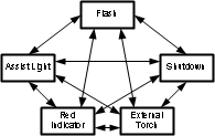
Table 1. Simple Mode Truth Table(1)
| EN1 | EN2 | TORCH | MODE |
|---|---|---|---|
| 0 | 0 | 0 | shutdown |
| 0 | 0 | 1 | external torch |
| 0 | 1 | X | assist light |
| 1 | 0 | X | indicator |
| 1 | 1 | X | flash |
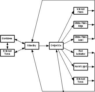 Figure 40. I2C Control State Diagram
Table 2. I2C Mode Truth Table(1)
| OEN | OM1 | OM0 | TEN | SEN | TORCH | STROBE | MODE |
|---|---|---|---|---|---|---|---|
| 0 | 0 | 0 | 0 | X | X | X | standby |
| 0 | 0 | 0 | 1 | X | 0 | X | standby |
| 0 | 0 | 0 | 1 | X | 1 | X | external torch |
| 0 | 0 | 1 | X | X | X | X | atandby |
| 0 | 1 | 0 | X | X | X | X | atandby |
| 0 | 1 | 1 | X | X | X | X | atandby |
| 1 | 0 | 0 | X | X | 0 | X | atandby |
| 1 | 0 | 0 | X | X | 1 | X | external torch |
| 1 | 0 | 1 | X | X | X | X | indicator |
| 1 | 1 | 0 | X | X | X | X | assist |
| 1 | 1 | 1 | X | 0 | X | X | internal flash |
| 1 | 1 | 1 | X | 1 | X | 0 | atandby |
| 1 | 1 | 1 | X | 1 | X | 1 | strobe flash |
7.5 Programming
7.5.1 I2C-Compatible Interface
7.5.1.1 Data Validity
The data on SDA line must be stable during the HIGH period of the clock signal (SCL). In other words, the state of the data line can only be changed when CLK is LOW.
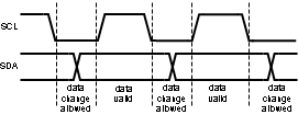 Figure 41. Data Validity Diagram
A pullup resistor between VIO and SDA must be greater than (VIO – VOL) / 3 mA to meet the VOL requirement on SDA. Using a larger pullup resistor results in lower switching current with slower edges, while using a smaller pullup results in higher switching currents with faster edges.
7.5.1.2 Start and Stop Conditions
START and STOP conditions classify the beginning and the end of the I2C session. A START condition is defined as SDA signal transitioning from HIGH to LOW while SCL line is HIGH. A STOP condition is defined as the SDA transitioning from LOW to HIGH while SCL is HIGH. The I2C master always generates START and STOP conditions. The I2C bus is considered to be busy after a START condition and free after a STOP condition. During data transmission, the I2C master can generate repeated START conditions. First START and repeated START conditions are equivalent, function-wise. The data on SDA line must be stable during the HIGH period of the clock signal (SCL). In other words, the state of the data line can only be changed when CLK is LOW.
 Figure 42. Start and Stop Conditions
7.5.1.3 Transferring Data
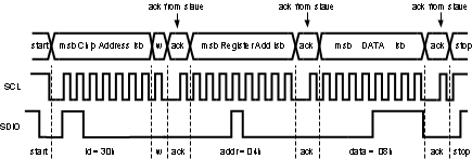
Every byte put on the SDA line must be eight bits long, with the most significant bit (MSB) being transferred first. Each byte of data has to be followed by an acknowledge bit. The acknowledge related clock pulse is generated by the master. The master releases the SDA line (HIGH) during the acknowledge clock pulse. The LM3555 pulls down the SDA line during the 9th clock pulse, signifying an acknowledge. The LM3555 generates an acknowledge after each byte has been received.
After the START condition, the I2C master sends a chip address. This address is seven bits long followed by an eighth bit which is a data direction bit (R/W). The LM3555 address is 30h. For the eighth bit, a 0 indicates a WRITE and a 1 indicates a READ. The second byte selects the register to which the data is written. The third byte contains data to write to the selected register.
7.5.1.4 I2C-Compatible Chip Address
The chip address for LM3555 is 0110000, or 30hex.
 Figure 44. Device Address
7.6 Register Maps
7.6.1 Internal Registers of LM3555
| REGISTER | INTERNAL HEX ADDRESS | POWER ON VALUE |
|---|---|---|
| Version Control Register | 0x01 | 0000 1100 |
| Indicator and Timer Register | 0x02 | 0000 1111 |
| Current Set Register | 0x03 | 0110 1001 |
| Control Register | 0x04 | 1011 0100 |
| Fault Register | 0x05 | 0000 1000 |
7.6.2 Register Definitions

DR3–DR0: design revision = 1100

VO1-VO0: VREF offset adjustment bits. used for diode detection.
FT3-FT0: software flash timer duration control bits
Table 3. Indicator Currents
| IC1 | IC0 | INDICATOR LED CURRENT |
|---|---|---|
| 0 | 0 | 2.5 mA |
| 0 | 1 | 5 mA |
| 1 | 0 | 7.5 mA |
| 1 | 1 | 10.0 mA |
Table 4. Offset Voltages
| VO1 | VO0 | VREFVOLTAGE (OFFSET FROM 4.35 V) |
|---|---|---|
| 0 | 0 | 4.35 V (+0 V) |
| 0 | 1 | 4.65 V (+0.3 V) |
| 1 | 0 | 4.05 V (−0.3 V) |
| 1 | 1 | 4.95 V (+0.6 V) |
Table 5. Flash Timeout Duration
| FT3 | FT2 | FT1 | FT0 | FLASH TIMEOUT DURATION |
|---|---|---|---|---|
| 0 | 0 | 0 | 0 | 100 ms |
| 0 | 0 | 0 | 1 | 150 ms |
| 0 | 0 | 1 | 0 | 200 ms |
| 0 | 0 | 1 | 1 | 250 ms |
| 0 | 1 | 0 | 0 | 300 ms |
| 0 | 1 | 0 | 1 | 350 ms |
| 0 | 1 | 1 | 0 | 400 ms |
| 0 | 1 | 1 | 1 | 450 ms |
| 1 | 0 | 0 | 0 | 500 ms |
| 1 | 0 | 0 | 1 | 550 ms |
| 1 | 0 | 1 | 0 | 600 ms |
| 1 | 0 | 1 | 1 | 650 ms |
| 1 | 1 | 0 | 0 | 700 ms |
| 1 | 1 | 0 | 1 | 750 ms |
| 1 | 1 | 1 | 0 | 800 ms |
| 1 | 1 | 1 | 1 | 850 ms |

DEN: diode detection enable bit. 1 = en, 0 = disabled. default = 1 (enabled)
AC2-AC0: assist light current control bits
Table 6. Flash Current Levels
| FC3 | FC2 | FC1 | FC0 | FLASH CURRENT LEVEL |
|---|---|---|---|---|
| 0 | 0 | 0 | 0 | 200 mA |
| 0 | 0 | 0 | 1 | 220 mA |
| 0 | 0 | 1 | 0 | 240 mA |
| 0 | 0 | 1 | 1 | 260 mA |
| 0 | 1 | 0 | 0 | 280 mA |
| 0 | 1 | 0 | 1 | 300 mA |
| 0 | 1 | 1 | 0 | 320 mA (2 LEDs) |
| 0 | 1 | 1 | 1 | 340 mA |
| 1 | 0 | 0 | 0 | 360 mA |
| 1 | 0 | 0 | 1 | 380 mA |
| 1 | 0 | 1 | 0 | 400 mA (2 LED maximum) |
| 1 | 0 | 1 | 1 | 420 mA |
| 1 | 1 | 0 | 0 | 440 mA |
| 1 | 1 | 0 | 1 | 460 mA |
| 1 | 1 | 1 | 0 | 480 mA |
| 1 | 1 | 1 | 1 | 500 mA (1LED) |
Table 7. Assist Light Current Levels
| AC2 | AC1 | AC0 | ASSIST CURRENT LEVEL |
|---|---|---|---|
| 0 | 0 | 0 | 60 mA |
| 0 | 0 | 1 | 60 mA (2 LEDs) |
| 0 | 1 | 0 | 60 mA |
| 0 | 1 | 1 | 80 mA (1 LED) |
| 1 | 0 | 0 | 100 mA |
| 1 | 0 | 1 | 120 mA |
| 1 | 1 | 0 | 140 mA |
| 1 | 1 | 1 | 160 mA |

SSU: strobe signal usage. 0 = edge sensitive, 1 = level sensitive. 1 = default
TEN: external torch mode enable. 0 = not allowed, 1 = allowed. 1 = default
OEN: output enable. 0 = output disabled, 1 = output enabled. 0 = default
SEN: strobe signal mode. 0 = disabled, 1 = enabled. 1 = default
OM1-OM0: output mode select bits
Table 8. Peak Inductor Current Limit Levels
| IL1 | IL0 | PEAK INDUCTOR CURRENT LIMIT |
|---|---|---|
| 0 | 0 | 1.25 A |
| 0 | 1 | 1.5 A |
| 1 | 0 | 1.75 A |
| 1 | 1 | 2 A |
Table 9. Output Modes
| OM1 | OM0 | OUTPUT MODE |
|---|---|---|
| 0 | 0 | external torch |
| 0 | 1 | indicator |
| 1 | 0 | assist light |
| 1 | 1 | flash |

SC: short-circuit fault: 1 = Fault, 0 = no fault
OTP: overtemperature protection fault. 1 = fault, 0 = no fault
TO: flash timeout fault. 1 = fault, 0 = no fault
DN: number of LEDs. 1 = 2 LEDs, 0 = 1 LED. (This bit is R/W). 1 = fault, 0 = no fault
IF: indicator LED fault. 1 = fault, 0 = no fault
IP: inductor peak current limit fault (broken inductor fault). 1 = fault, 0 = no fault
RFU: not used