SNVS594G December   2008  – April 2016 LM3555

PRODUCTION DATA.  

  1. Features
  2. Applications
  3. Description
  4. Revision History
  5. Pin Configuration and Functions
  6. Specifications
    1. 6.1 Absolute Maximum Ratings
    2. 6.2 ESD Ratings
    3. 6.3 Recommended Operating Conditions
    4. 6.4 Thermal Information
    5. 6.5 Electrical Characteristics
    6. 6.6 Control Interface Timing Requirements
    7. 6.7 Typical Characteristics
  7. Detailed Description
    1. 7.1 Overview
    2. 7.2 Functional Block Diagram
    3. 7.3 Feature Description
      1. 7.3.1  Synchronous Boost Converter
      2. 7.3.2  High-Side Current Source
      3. 7.3.3  I2C/EN Pin
      4. 7.3.4  SDA/EN2 and SCL/EN1 Pins
      5. 7.3.5  STROBE Pin
      6. 7.3.6  TORCH Pin
      7. 7.3.7  Indicator LED Pin (IND)
      8. 7.3.8  Internal Diode Detection
      9. 7.3.9  Fault Protections
        1. 7.3.9.1 Output Overvoltage Protection (OVP)
        2. 7.3.9.2 Output and LED Short-Circuit Protection (SCP)
        3. 7.3.9.3 Overtemperature Protection (OTP)
        4. 7.3.9.4 Flash Timeout (FTP)
        5. 7.3.9.5 Indicator Fault (IF)
        6. 7.3.9.6 Broken Inductor Fault (IP)
      10. 7.3.10 Undervoltage Lockout (UVLO)
      11. 7.3.11 Power-On Reset (POR)
    4. 7.4 Device Functional Modes
      1. 7.4.1 Single LED Operation
      2. 7.4.2 Dual LED Operation
      3. 7.4.3 Torch or Assist (Continuous Current) Operation
      4. 7.4.4 Flash (Pulsed Current) Operation
      5. 7.4.5 Indicator Operation
      6. 7.4.6 Simple Control State Diagram
    5. 7.5 Programming
      1. 7.5.1 I2C-Compatible Interface
        1. 7.5.1.1 Data Validity
        2. 7.5.1.2 Start and Stop Conditions
        3. 7.5.1.3 Transferring Data
        4. 7.5.1.4 I2C-Compatible Chip Address
    6. 7.6 Register Maps
      1. 7.6.1 Internal Registers of LM3555
      2. 7.6.2 Register Definitions
  8. Application and Implementation
    1. 8.1 Application Information
    2. 8.2 Typical Application
      1. 8.2.1 Design Requirements
      2. 8.2.2 Detailed Design Procedure
        1. 8.2.2.1 Inductor Current Limit
        2. 8.2.2.2 Inductor Selection
        3. 8.2.2.3 Capacitor Selection
      3. 8.2.3 Application Curves
  9. Power Supply Recommendations
  10. 10Layout
    1. 10.1 Layout Guidelines
    2. 10.2 Layout Example
  11. 11Device and Documentation Support
    1. 11.1 Device Support
      1. 11.1.1 Third-Party Products Disclaimer
    2. 11.2 Documentation Support
      1. 11.2.1 Related Documentation
    3. 11.3 Community Resources
    4. 11.4 Trademarks
    5. 11.5 Electrostatic Discharge Caution
    6. 11.6 Glossary
  12. 12Mechanical, Packaging, and Orderable Information

Package Options

Mechanical Data (Package|Pins)
Thermal pad, mechanical data (Package|Pins)
Orderable Information

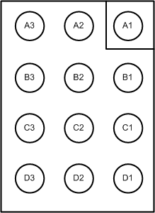
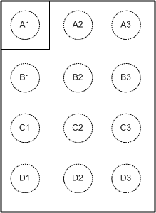
5 Pin Configuration and Functions

YZR Package
12-Pin DSBGA
Top View
LM3555 connection_top.gif
YZR Package
12-Pin DSBGA
Bottom View
LM3555 connection_bottom.gif

Pin Functions

PIN I/O DESCRIPTION
NUMBER NAME
A1 PGND Power ground
A2 SGND Signal ground
A3 VIN I Input voltage pin of the device. Connect input bypass capacitor very close to this pin.
B1 SW Inductor connection
B2 TORCH I Torch pin. Driving this pin high enables torch mode.
B3 IND O Red indicator LED current source. Connect to RED LED anode
C1 VOUT O Boost output. Connect output bypass capacitor very close to this pin
C2 STROBE I/O Strobe signal input pin to synchronize flash pulse in I2C mode. This signal usually comes from the camera processor. In simple logic mode this pin, when tied to a voltage rail through a pullup resistor indicates the number of LEDs in the system.
C3 I2C / EN I I2C / EN-logic selection. High = I2C mode, Low = simple logic mode.
D1 VLED O LED current source. Connect to the anode of the flash LED. One or two LEDs can be connected in series.
D2 SDA / EN2 I/O EN2 signal pin in simple logic mode. I2C data signal in I2C mode.
D3 SCL / EN1 I EN1 signal pin in simple logic mode. I2C clock signal in I2C mode.