SNVS594G December   2008  – April 2016 LM3555

PRODUCTION DATA.  

  1. Features
  2. Applications
  3. Description
  4. Revision History
  5. Pin Configuration and Functions
  6. Specifications
    1. 6.1 Absolute Maximum Ratings
    2. 6.2 ESD Ratings
    3. 6.3 Recommended Operating Conditions
    4. 6.4 Thermal Information
    5. 6.5 Electrical Characteristics
    6. 6.6 Control Interface Timing Requirements
    7. 6.7 Typical Characteristics
  7. Detailed Description
    1. 7.1 Overview
    2. 7.2 Functional Block Diagram
    3. 7.3 Feature Description
      1. 7.3.1  Synchronous Boost Converter
      2. 7.3.2  High-Side Current Source
      3. 7.3.3  I2C/EN Pin
      4. 7.3.4  SDA/EN2 and SCL/EN1 Pins
      5. 7.3.5  STROBE Pin
      6. 7.3.6  TORCH Pin
      7. 7.3.7  Indicator LED Pin (IND)
      8. 7.3.8  Internal Diode Detection
      9. 7.3.9  Fault Protections
        1. 7.3.9.1 Output Overvoltage Protection (OVP)
        2. 7.3.9.2 Output and LED Short-Circuit Protection (SCP)
        3. 7.3.9.3 Overtemperature Protection (OTP)
        4. 7.3.9.4 Flash Timeout (FTP)
        5. 7.3.9.5 Indicator Fault (IF)
        6. 7.3.9.6 Broken Inductor Fault (IP)
      10. 7.3.10 Undervoltage Lockout (UVLO)
      11. 7.3.11 Power-On Reset (POR)
    4. 7.4 Device Functional Modes
      1. 7.4.1 Single LED Operation
      2. 7.4.2 Dual LED Operation
      3. 7.4.3 Torch or Assist (Continuous Current) Operation
      4. 7.4.4 Flash (Pulsed Current) Operation
      5. 7.4.5 Indicator Operation
      6. 7.4.6 Simple Control State Diagram
    5. 7.5 Programming
      1. 7.5.1 I2C-Compatible Interface
        1. 7.5.1.1 Data Validity
        2. 7.5.1.2 Start and Stop Conditions
        3. 7.5.1.3 Transferring Data
        4. 7.5.1.4 I2C-Compatible Chip Address
    6. 7.6 Register Maps
      1. 7.6.1 Internal Registers of LM3555
      2. 7.6.2 Register Definitions
  8. Application and Implementation
    1. 8.1 Application Information
    2. 8.2 Typical Application
      1. 8.2.1 Design Requirements
      2. 8.2.2 Detailed Design Procedure
        1. 8.2.2.1 Inductor Current Limit
        2. 8.2.2.2 Inductor Selection
        3. 8.2.2.3 Capacitor Selection
      3. 8.2.3 Application Curves
  9. Power Supply Recommendations
  10. 10Layout
    1. 10.1 Layout Guidelines
    2. 10.2 Layout Example
  11. 11Device and Documentation Support
    1. 11.1 Device Support
      1. 11.1.1 Third-Party Products Disclaimer
    2. 11.2 Documentation Support
      1. 11.2.1 Related Documentation
    3. 11.3 Community Resources
    4. 11.4 Trademarks
    5. 11.5 Electrostatic Discharge Caution
    6. 11.6 Glossary
  12. 12Mechanical, Packaging, and Orderable Information

Package Options

Mechanical Data (Package|Pins)
Thermal pad, mechanical data (Package|Pins)
Orderable Information

10 Layout

10.1 Layout Guidelines

The DSBGA is a chip-scale package with good thermal properties. For more detailed instructions on handling and mounting DSBGA packages, refer to AN-1112 DSBGA Wafer Level Chip Scale Package (SNVA009).

The high switching frequencies and large peak currents make the PCB layout a critical part of the design. The proceeding steps must be followed to ensure stable operation and proper current source regulation.

  1. Connect the inductor as close to the SW pin as possible. This reduces the inductance and resistance of the switching node which minimizes ringing and excess voltage drops.
  2. Connect the return terminals of the input capacitor and the output capacitor as close to the two ground pins (PGND and SGND) as possible and through low impedance traces.
  3. Bypass VIN with a 10-µF ceramic capacitor and an additional 0.1-µF ceramic capacitor. Connect the positive terminal of this capacitor as close to VIN as possible.
  4. Connect COUT as close to the VOUT pin as possible. This reduces the inductance and resistance of the output bypass node which minimizes ringing and voltage drops. This improves efficiency and decreases the noise injected into the current sources.

10.2 Layout Example
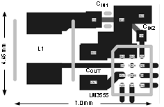
LM3555 30079476.gif Figure 58. LM3555 Layout