SNVS834 August 2014 LM3631
PRODUCTION DATA.
- 1 Features
- 2 Applications
- 3 Description
- 4 Revision History
- 5 Device Comparison Table
- 6 Pin Configuration and Functions
- 7 Specifications
-
8 Detailed Description
- 8.1 Overview
- 8.2 Functional Block Diagram
- 8.3 Features Description
- 8.4 Device Functional Modes
- 8.5 Programming
- 8.6 Register Maps
- 9 Application and Implementation
- 10Power Supply Recommendations
- 11Layout
- 12Device and Documentation Support
- 13Mechanical, Packaging, and Orderable Information
Package Options
Mechanical Data (Package|Pins)
- YFF|24
Thermal pad, mechanical data (Package|Pins)
Orderable Information
9 Application and Implementation
9.1 Application Information
The LM3631 integrates an LCD backlight driver and LCD positive and negative bias voltage supplies into a single device. The backlight boost converter generates the high voltage required for the LEDs. The LM3631 can drive one or two LED strings with 4 to 8 white LEDs per string. Positive and negative bias voltages are post-regulated from the LCD bias boost output voltage. In addition, for the LCD bias voltages, the device has two programmable LDO regulator outputs which can be used to the power display controller, the LCD gamma reference, or any additional peripherals within output-current capability.
LDC bias voltages can be used without the backlight. Pulling LCD_EN high starts the LCD bias boost regulator. Once the LCD bias boost regulator has started up all voltage outputs can be enabled individually. The LM3631 can also be programmed to enable any voltage outputs automatically per a preset start-up sequence. The backlight cannot be enabled until enabled bias voltages have settled.
9.2 Typical Application
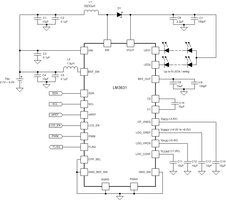 Figure 58. Typical Application Schematic
9.2.1 Design Requirements
Example requirements based on default register values (OTP_SEL = 1):
| DESIGN PARAMETER | EXAMPLE VALUE |
|---|---|
| Input Voltage Range | 2.7 V to 4.5 V (Single Li-Ion cell battery) |
| Brightness Control | I2C Register |
| LED Configuration | 2 parallel, 6 series |
| LED Current | max 25 mA / string |
| Backlight Boost maximum voltage | 28 V |
| Backlight boost SW frequency | 1MHz |
| Backlight Boost inductor | 10-µH, 900-mA saturation current |
| LCD boost output voltage | 5.9 V |
| VNEG output voltage | –5.4 V |
| VPOS output voltage | 5.4 V |
| VOREF output voltage | 5.6 V |
| VCONT output voltage | 1.8 V |
| LCD Boost inductor | 1.5-µH, 1-A saturation current |
9.2.2 Detailed Design Procedure
9.2.2.1 External Components
Table 33 shows examples of external components for the LM3631. Small 100-pF ceramic capacitors parallel with boost-converter-output capacitors are optional and are used to reduce high-frequency noise generated by the boost converters. Boost-converter dual-output capacitors can be replaced with a single capacitor of higher output capacitance as long as the minimum effective capacitance requirement is met. DC bias effect of the ceramic capacitors must be taken into consideration when choosing the output capacitors. This is especially true for the high output-voltage backlight-boost converter.
Table 33. Recommended External Components
| DESIGNATOR (Figure 58) | DESCRIPTION | VALUE | EXAMPLE | NOTE |
|---|---|---|---|---|
| C1, C4, C8, C10, C11, C12, C13, C14 | Ceramic capacitor | 10 µF, 10V or 16V | EMK107BBJ106MA-T | |
| C2, C3, C5 | Ceramic capacitor | 0.1 µF, 10V | GRM188R71H104KA93D | |
| C6 | Ceramic capacitor | 2.2 µF, 35V or 50V | C2012X5R1H225K | |
| C7, C9 | Ceramic capacitor | 100 pF, 50V | 06035A101JAT2A | Optional, only for HF interference reduction. |
| L1 | Inductor | 22 or 10 µH, 900mA | VLF403210MT-100M or 1235AS-H-220M | |
| L2 | Inductor | 1.5 µH | DFE252010R-H-1R5M | |
| D1 | Schottky diode | 40V, 200mA | NSR0240P2T5G |
9.2.2.2 Inductor Selection
Both of the LM3631 boost converters are internally compensated. The compensation parameters of the LCD bias boost converter are fixed and set for a 1.5-µH inductor. The backlight boost converter has a selection bit to choose between 10-µH or 22-µH inductors. The inductor typical inductance is selected with the INDUCTOR bit (Register 0x06, bit 2). Effective inductance of the inductors should be ±20%.
There are two main considerations when choosing an inductor: the inductor should not saturate, and the inductor current ripple should be small enough to achieve the desired output voltage ripple. Different saturation current rating specifications are followed by different manufacturers so attention must be given to details. Saturation current ratings are typically specified at 25°C. However, ratings at the maximum ambient temperature of application should be requested from the manufacturer. The saturation current should be greater than the sum of the maximum load current and the worst-case average-to-peak inductor current. The equation below shows the worst case conditions.
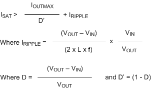
where
- IRIPPLE = peak inductor current
- IOUTMAX = maximum load current
- VIN = minimum input voltage in application
- L = minimum inductor value including worst case tolerances
- f = minimum switching frequency
- VOUT = output voltage
As a result the inductor should be selected according to the ISAT. A more conservative and recommended approach is to choose an inductor that has a saturation current rating greater than the maximum current limit. The inductor’s resistance should be kept small for good efficiency.
See detailed information in “Understanding Boost Power Stages in Switch Mode Power Supplies” http://focus.ti.com/lit/an/slva061/slva061.pdf. “Power Stage Designer™ Tools” can be used for the boost calculation: http://www.ti.com/tool/powerstage-designer.
9.2.2.3 Boost Output Capacitor Selection
Two 2.2-μF capacitors are recommended for the backlight boost converter output capacitors. A single 2.2-μF capacitor can be used for reducing solution size as long as the effective output capacitance is higher than 1 µF. A high-quality ceramic type X5R or X7R is recommended. Voltage rating must be greater than the maximum output voltage that is used.
For the LCD-bias-boost output two 10-μF capacitors are recommended. A high-quality ceramic type X5R or X7R is recommended. Voltage rating must be greater than the maximum output voltage that is used.
The DC-bias effect of the capacitors must be taken into consideration when selecting the output capacitors. The effective capacitance of a ceramic capacitor can drop down to less than 10% with maximum rated DC bias voltage depending on capacitor type. Note that with a same voltage applied, the capacitors with higher voltage rating suffer less from the DC-bias effect than capacitors with lower voltage rating.
9.2.2.4 Backlight Boost Diode Selection
A Schottky diode should be used for the output diode. Peak repetitive current should be greater than inductor peak current to ensure reliable operation. Average current rating should be greater than the maximum output current. Reverse breakdown voltage of the Schottky diode should be significantly larger than the maximum output voltage.
9.2.2.5 Charge Pump Capacitor Selection
Voltage ratings for the flying capacitor and output capacitor must be higher than the maximum output voltage. Ceramic X5R/X7R capacitors are recommended. 10-V voltage rating and 10 µF capacitors are recommended for both.
9.2.2.6 LDO Output Capacitor Selection
Voltage ratings for the LDO output capacitors must be higher than the maximum output voltage. Ceramic X5R/X7R capacitors are recommended. 10-V voltage rating and 10-µF capacitors are recommended for all.
9.2.3 Application Curves
Figure 59 and Figure 60 show typical backlight start-up and shutdown curves using the LCD_EN pin control.
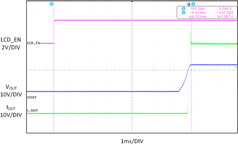 Figure 59. Backlight Start-up with LCD_EN Pin Control
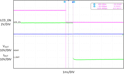 Figure 60. Backlight Shutdown with LCD_EN Pin Control
Figure 61 and Figure 62 show the default start-up and shutdown waveforms with OTP_SEL = GND. LDO_CONT pulldown is disabled by default causing VCONT to float after shutdown.
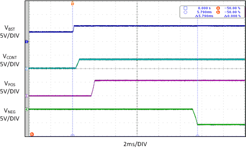 Figure 61. Default LCD Bias Startup, OTP_SEL = GND.
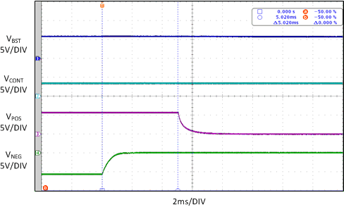 Figure 62. Default LCD Bias Shutdown, OTP_SEL = GND.