SNVS834 August 2014 LM3631
PRODUCTION DATA.
- 1 Features
- 2 Applications
- 3 Description
- 4 Revision History
- 5 Device Comparison Table
- 6 Pin Configuration and Functions
- 7 Specifications
-
8 Detailed Description
- 8.1 Overview
- 8.2 Functional Block Diagram
- 8.3 Features Description
- 8.4 Device Functional Modes
- 8.5 Programming
- 8.6 Register Maps
- 9 Application and Implementation
- 10Power Supply Recommendations
- 11Layout
- 12Device and Documentation Support
- 13Mechanical, Packaging, and Orderable Information
Package Options
Mechanical Data (Package|Pins)
- YFF|24
Thermal pad, mechanical data (Package|Pins)
Orderable Information
8 Detailed Description
8.1 Overview
The LM3631 is a single-chip complete LCD power and backlight solution. It can drive up to two LED strings with up to 8 LEDs each (up to 27 V typ.), with a maximum of 25 mA per string. The power for the LED strings comes from a integrated asynchronous backlight boost converter with two selectable switching frequencies (500 kHz or 1 MHz) to optimize performance or solution area. LED current is regulated by two low-headroom current sinks. Automatic voltage scaling adjust the output voltage of the backlight boost converter to minimize the LED driver head room voltage.
The LCD bias power portion of the LM3631 consists of an LCD bias boost converter, inverting charge pump, and three integrated LDOs. The device can generate all the required voltages for a LCD panel:
- The LCD positive bias voltage VPOS (up to 6V). VPOS voltage is post-regulated from the LCD bias boost converter output voltage.
- LCD negative bias voltage VNEG (down to –6 V). VNEG is generated from the LCD bias boost converter output using a regulated inverting charge pump.
- The third output VOREF can supply the LCD gamma (or VCOM reference) voltage. VOREF is post-regulated from the LCD bias boost converter output voltage.
- The fourth output VCONT can be used to supply the display controller. VCONT regulator is powered from the VIN input.
The LM3631 flexible control interface consists from nRST active low reset input, LCD_EN enable input, PWM input for content adaptive backlight control (CABC), and an I2C-compatible interface. In applications with limited IO pin count the LCD_EN input pin function can be replaced with the LCD_EN I2C register bit. In this case the LCD_EN pin needs to be connected to ground. OTP_SEL input can be used to select from two different factory-programmed default One Time Programmable Memory (OTP) settings. The default OTP settings can be overwritten using the I2C-compatible interface. Programmable settings include LED ramp up/down profiles, LED output current and brightness control modes, enabling/disabling individual power supply outputs, and programmable LCD output power up/down sequencing. Open drain FLAG output can be used to notify host processor from various power-good signals or fault conditions.
 Figure 38. System Example
8.2 Functional Block Diagram
8.3 Features Description
8.3.1 Backlight
The backlight is enabled by setting the BL_EN = 1 and a brightness value higher than zero. LCD bias power rails need to reach their target voltages before the backlight can be started. Note that all bias voltages don't need to be enabled to start up the backlight. For example, if only VPOS and VNEG are required, the backlight can be enabled once these voltages have reach their target voltages. In this case VCONT and VOREF can be disabled. If all four outputs (LDO_CONT, LDO_OREF, CP_VNEG, and LDO_VPOS) are disabled, the backlight can be enabled once the LCD biast boost converter has settled. The LCD bias boost is always enabled when the LCD_EN pin or bit is set high.
When the brightness value is '0', or BL_EN bit is ‘0’, the backlight is disabled. The BL_EN bit is '1' by default. The backlight can be disabled at any time by setting the brightness value to zero or by writing the BL_EN bit to ‘0’.
LED driver LED2 can be separately enabled and disabled from the I2C register. LED driver LED1 is always enabled when the backlight is turned on.
Table 2. Backlight Control
| BL_EN BIT | BRIGHTNESS VALUE (I2C AND/OR EXTERNAL PWM) | BACKLIGHT ON/OFF |
|---|---|---|
| 0 | 0 | OFF |
| 0 | ≥1 | OFF |
| 1 | 0 | OFF |
| 1 | ≥1 | ON |
8.3.1.1 Backlight Brightness Control
Brightness can be controlled either by the I2C brightness register, with an external PWM control, or a combination of both. BRT_MODE bits select the brightness control mode. Different brightness control modes are shown in Table 3.
When controlling brightness through I2C, registers 0x01 and 0x02 are used. Registers 0x01 and 0x02 hold the 11-bit brightness data. Register 0x02 contains the 8 MSBs, and register 0x01 contains the 3 LSBs. The LED current only transitions to the new level after a write is done to register 0x02.
When controlling brightness through I2C, setting brightness value to '0' shuts down the backlight. When controlling the brightness with PWM input, if PWM input is low for a certain period of time (24 ms typ.), the backlight shuts down. When using the combination of a PWM input and the I2C register, either option shuts down the backlight.
NOTE
The backlight does not start before the LCD bias start-up sequence is finished even if BL_EN bit is '1' and the brightness setting is ≥ 1.
Table 3. Brightness Control
| BRT_MODE bits | BRIGHTNESS CONTROL |
|---|---|
| 00 | I2C register used for brightness control |
| 01 | PWM input duty cycle used for brightness control |
| 10 | I2C register code multiplied with PWM duty cycle before sloping |
| 11 | Sloped I2C register code multiplied with PWM duty cycle |
 Figure 39. Brightness Control with
 BRT_MODE bit 00
 Figure 41. Brightness Control with
 BRT_MODE bit 10
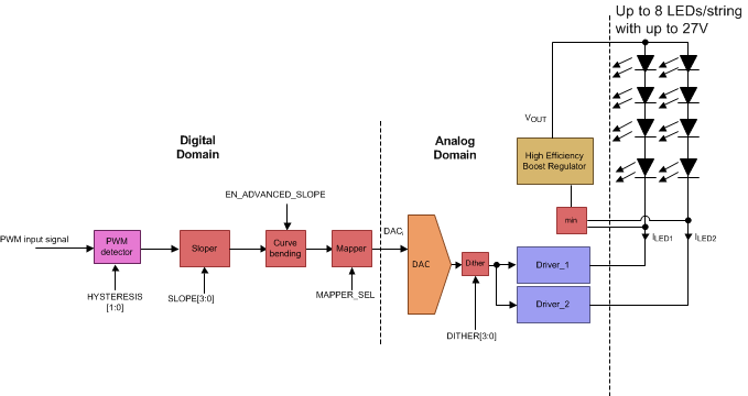 Figure 40. Brightness Control with
 BRT_MODE bit 01
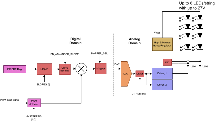 Figure 42. Brightness Control with
 BRT_MODE bit 11
8.3.1.1.1 LED Current With Brightness Selection '00'
When LED brightness is controlled from the I2C brightness registers, the 11-bit brightness data directly controls the LED current in LED1 and LED2. LED mapping can be selected as either linear or exponential. When this mode is selected setting PWM input to 0 does not disable the backlight.
With exponential mapping the 11-bit code-to-current response is approximated by the equation:
This equation is valid for I2C brightness codes between 1 and 2047. Code 0 disables the backlight. Resolution achieved at the output is maximum 16-bit at low brightness levels and additional 1 bit can be achieved with the dithering resulting in up to 17-bit output resolution. Step sizes increase when the current increases with the exponential control.
Figure 43 and Figure 44 detail the exponential response of the LED current vs. brightness code. Figure 43 shows the response on a linear Y axis while Figure 44 shows the response on a log Y axis to show the low current levels at the lower codes.
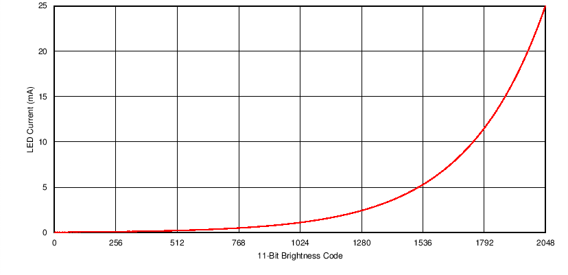 Figure 43. Exponential Response of the LED Current vs Brightness Code
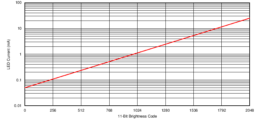 Figure 44. Response of the LED Current vs Brightness Code on a Log Y Axis
With linear mapping the 11-bit code to current response is approximated by the equation:
This equation is valid for codes between 1 and 2047. Code 0 disables the backlight.
8.3.1.1.2 LED Current With Brightness Selection '01'
When LED brightness is controlled from the PWM, the PWM duty cycle directly controls the LED current in LED1 and LED2. LED mapping can be selected to be either linear or exponential. When this mode is selected, setting the I2C brightness register to 0 does not disable the backlight.
With exponential mapping the PWM duty cycle-to-current response is approximated by the equation:
Equation 3 is valid for PWM duty cycles other than 0. Duty cycle 0 disables the backlight.
With linear mapping the PWM duty cycle-to-current response is approximated by the equation:
Equation 4 is valid for PWM duty cycles other than 0. Duty cycle 0 disables the backlight.
8.3.1.1.3 LED Current With Brightness Selections '10' and '11'
When LED brightness is controlled with the combination of the I2C register and the PWM duty cycle, the multiplication result of I2C register value and PWM duty cycle controls the LED current in LED1 and LED2. LED mapping can be selected as either linear or exponential.
With exponential mapping the multiplication result-to-current response is approximated by the equation:
Equation 5 is valid for brightness values other than 0. Brightness value (PWM D/C or I2C BRT CODE) 0 disables the backligh.
With linear mapping the PWM duty cycle-to-current response is approximated by the equation:
Equation 6 is valid for brightness values other than 0. Brightness value (PWM D/C or I2C BRT CODE) 0 programs 0 current.
The key difference between the two brightness modes is how the PWM input affects the LED output current. When brightness mode is '10', changing PWM value causes LED current to slope form the current value to the new value. With the brightness setting '11', a change in PWM value causes an instant change in the LED current. This makes brightness setting '11' suitable for CABC operation.
8.3.1.2 Linear Slope and Advanced Slope
Sloper smooths the transition from one brightness value to another. Slope time can be adjusted from 0 ms to 4000 ms with SLOPE[3:0] bits. Slope time is used for sloping up and down. Slope time always remains the same regardless of the amount of change in brightness. Advanced slope makes brightness changes smooth for the human eye.
Dithering function further smooths the slope by jumping between two adjacent current values. Dithering frequency can be programmed with DITHER_FREQ_SEL[3:0] bits. Dithering function can be disabled with DISABLE_DITHER bit.
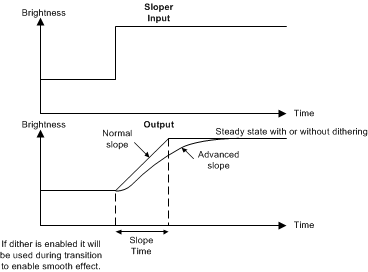 Figure 45. Sloper
Table 4. Slope Times
| SLOPE BITS[3:0] | SLOPE TIME (ms) |
|---|---|
| 0000 | 0, slope function disabled, immediate brightness change |
| 0001 | 1 |
| 0010 | 2 |
| 0011 | 5 |
| 0100 | 10 |
| 0101 | 20 |
| 0110 | 50 |
| 0111 | 100 |
| 1000 | 250 |
| 1001 | 500 |
| 1010 | 750 |
| 1011 | 1000 |
| 1100 | 1500 |
| 1101 | 2000 |
| 1110 | 3000 |
| 1111 | 4000 |
8.3.1.3 Mapper
The mapper block maps the digital word into current code which is set for the LED driver. The user can select whether the mapping is exponential or linear with the LINEAR_MAPPER bit.
Exponential control is tailored to the response of the human eye such that the perceived change in brightness during ramp up or ramp down is linear.
8.3.1.4 PWM Detector and PWM Input
The PWM detector block measures the duty cycle in the PWM pin. The PWM period is measured from the rising/falling edge to the next rising/falling edge. PWM edge detection can be selected as rising or falling from register 0x08 bit 7. PWM polarity can be changed with register 0x08 bit 6. The PWM input block timeout is 24 ms after the last rising edge, which should be taken into account for 0% and 100% brightness settings (for setting 100% brightness, high level of PWM input signal should be at least 24 ms). Minimum on and off times for PWM input signal are 400 ns.
PWM input resolution is defined by the PWM detector sampling rate (24 MHz typ.). Resolution depends on the input signal frequency — for example, with 10-kHz PWM input frequency the resolution is 11-bit. If a higher input frequency is used, the resolution is lower. The minimum recommended PWM frequency is 100 Hz, and maximum recommended PWM frequency is 20 kHz.
PWM hysteresis selection sets the minimum allowable change to the input. If a smaller change is detected, it is ignored. With hysteresis the constant changing between two brightness values is avoided if there is small jitter in the input signal. Hysteresis is selected with HYSTERESIS bits in register 0x08. Using a higher hysteresis setting is recommended with high PWM input frequencies.
The PWM detector is disabled in I2C brightness mode to minimize current consumption.
8.3.2 Backlight Boost Converter
The LM3631 can drive two LED strings with up to 8 LEDs per string. The high voltage required by the LED strings is generated with an asynchronous backlight boost converter. An adaptive voltage control loop automatically adjusts the output voltage based on the voltage over the LED drivers LED1 and LED2.
The LM3631 has two switching frequency modes (high and low). These are set via the Boost Frequency Select bit. The nominal low- and high-frequency set points are 500 kHz and 1 MHz, respectively. Operation in low-frequency mode results in better efficiency at lighter load currents due to the decreased switching losses. Operation in high-frequency mode gives better efficiency at higher load currents due to the reduced inductor current ripple and the resulting lower conduction losses in the MOSFETs and inductor.
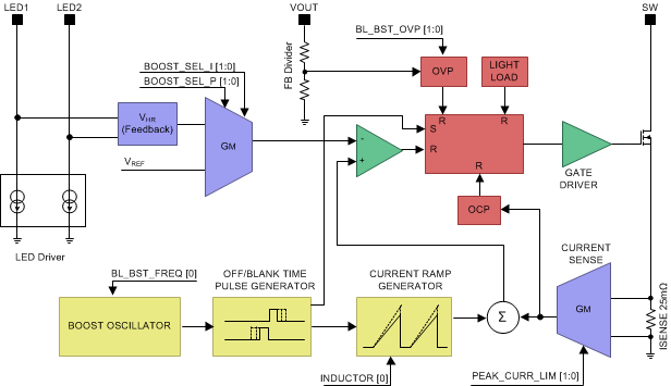 Figure 46. Backlight Boost Block Diagram
8.3.2.1 Headroom Voltage
Saturation voltage of the LED drivers depends on the output current setting. In order to optimize LED drive efficiency, while maintaining good LED current accuracy, the LED-driver-regulated headroom voltage (VHR) is kept slightly above LED driver saturation voltage. To maintain good LED current accuracy with lower current settings, LED driver size is scaled down for the lower current settings (below 1/16 of max current). In order to ensure that both current sinks remain in regulation when there is a mismatch in string voltages, the boost converter output voltage is regulated based on the LED driver with lower headroom voltage. For example, if the LEDs connected to LED1 require 25 V at the programmed current, and the LEDs connected to LED2 require 25.5 V at the programmed current, the voltage at LED1 is VHR + 0.5 V, and the voltage at LED2 is VHR.
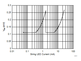 Figure 47. Regulated Headroom vs LED Current
8.3.2.2 Automatic Switching Frequency Shift
To take advantage of frequency vs load dependent losses, the LM3631 has an automatic frequency-select mode. In automatic frequency-select mode the switching-frequency bit is automatically changed based on the programmed LED current. The threshold (or LED Brightness Code) at which the frequency switchover occurs is programmable via the AUTOFREQ_THRESHOLD. This register contains an 8-bit code which is compared against the 8 MSB’s of the brightness code (BRT[10:3]). When BRT[10:3] > AUTOFREQ_THRESH[7:0], the Boost Frequency Select Bit is set to a ‘1’, and the device operates in high-frequency mode. When BRT[10:3] ≤ AUTOFREQ_THRESH[7:0], the Frequency Select Bit is automatically set to ‘0’, and the device operates in low-frequency mode.
When automatic frequency-select mode is disabled, the switching frequency operates at the programmed high- or low-frequency setting across the entire LED current range.
8.3.2.3 Inductor Select Bit
The LM3631 can operate with a 10-µH or 22-µH inductor. However, the LM3631 backlight boost-control loop requires adjustment of internal loop compensation parameters based on the inductance value selected for the application. This is done through the INDUCTOR bit. For 10-µH inductors, the INDUCTOR bit must be set to '1'. For a 22-µH inductor, the INDUCTOR bit should be set to ‘0’.
8.3.2.4 PI-Compensator
The LM3631 backlight boost converter internal loop-compensation parameters (SEL_I[1:0] and SEL_P[1:0]) are factory-selected to optimize performance and stability for most backlight configurations. These settings should not need adjustment. If these settings are changed, application needs to be carefully evaluated to ensure stability and performance in all operating conditions.
8.3.3 Backlight Protection and Faults
8.3.3.1 Overvoltage Protection (OVP) and Open-Load Fault Protection
The LM3631 provides an OVP that monitors the LED boost output voltage (VOUT) and protects OUT and SW from exceeding safe operating voltages. The OVP threshold can be set with the I2C register bits. The OVP limit can be set to 17 V, 21 V, 25 V, or 29 V. The OVP monitor differentiates between two overvoltage conditions and responds accordingly as outlined below:
-
Case 1 (OVP Threshold hit and (VLED1 and VLED2 ) > 40 mV):
In steady-state operation with VOUT near the OVP threshold (VOVP), a rapid change in VIN or brightness code can result in a momentary transient excursion of VOUT above the OVP threshold. In this case the boost circuitry is disabled until VOUT drops below VOVP - VHYST. Once this happens the boost is re-enabled, and steady state regulation can commence. If the OVP pulse length is over 1 ms, an OVP fault is set.
-
Case 2 (OVP Threshold hit and (VLED1 and VLED2 ) < 40 mV):
When one or all of the LED strings is open, the boost converter drives VOUT above VOVP and at the same time the open string(s) current sink headroom voltage(s) drops to 0. When LM3631 detects three pulses (if VOUT > VOVP and (VLED1 or VLED2) < 40 mV), the OVP Fault flag (BL_OVPFLT) is set. If the OVP pulse length is over 1 ms, an OVP fault is set. The flag is cleared with rising LCD_EN or an I2C write.
8.3.3.2 Overcurrent Protection (OCP) and Overcurrent Protection Fault
The LM3631 has 4 selectable OCP thresholds. The programmable options are 600 mA, 700 mA, 800 mA, or 900 mA. The OCP threshold is a cycle-by-cycle current limit detected in the low-side NFET. Once the threshold is reached, the NFET turns off for the remainder of the switching period.
8.3.3.2.1 Overcurrent Protection Fault Flag (BL_OCPFLT)
If enough OCP threshold events occur the Overcurrent Protection Fault (BL_OCPFLT) flag is set. To avoid transient conditions from inadvertently setting the BL_OCPFLT Flag, a Pulse Density Counter monitors OCP threshold events over a 128-µs period. If the Pulse Density Counter counts 2 or more OCP events during the 128-µs period, the pulse density count is considered true. If 8 consecutive 128-µs periods occur where the pulse density count is true (1024 µs total), the BL_OCPFLT fault is set. Fault is cleared by rising edge of the LCD_EN or an I2C write '1' to the BL_OCPFLT bit.
NOTE
The OCP signaling is ignored for 4 ms after the backlight boost is started or the brightness value is changed.
8.3.3.2.2 Short Circuit Fault Flag (BL_SCFLT)
If an OCP fault has occurred, and the headroom voltage is too low (VLED1 or VLED2 < 40 mV), the Short Circuit Fault (BL_SCFLT) fault is set, and all power is shut down. The fault must be cleared to enable power — it is cleared by the rising edge of the LCD_EN or by an I2C write '1' to the BL_SCFLT bit.
NOTE
The OCP signaling is ignored for 4 ms after the backlight boost is started or the brightness value is changed.
8.3.4 LCD Bias
8.3.4.1 Display Bias Power (VPOS, VNEG, VOREF)
A single high-efficiency boost converter provides a positive voltage rail, VBST_OUT, which serves as the power rail for the LCD VPOS and VNEG biases, as well as for an additional regulated output VOREF. This can be used to supply the display gamma reference, VCOM and VCS voltages.
- The VPOS output LDO, LDO_VPOS, has a programmable range from 4 V up to 6 V with 50-mV steps and can supply up to 100 mA.
- The VNEG output, CP_VNEG, is generated from a regulated, inverting charge pump and has an adjustable range of –6 V up to –4 V with 50-mV steps and a maximum load of 80 mA. During start-up there is a minimum delay of 500 µs due to biasing the flycap.
- The VOREF output LDO, LDO_OREF, has programmable range from 4 V to 6 V, further adjustable in 50-mV increments and can supply up to 50 mA.
The boost voltage can be selected from the an I2C register. When selecting suitable boost-output voltage, the following estimation can be used VBST = max(VLDO_VPOS, |VCP_VNEG|,VLDO_OREF) + 200 mV (with lower currents) or + 300 mV (with higher currents). When the device input voltage (VIN) > sets the LCD boost output voltage, the boost voltage goes to VIN + 100 mV.
Table 5. LCD Boost VOUT
| LCD_BOOST_VOUT BITS | LCD BOOST OUTPUT VOLTAGE (V) |
|---|---|
| 000 000 | 4.50 |
| 000 001 | 4.55 |
| 000 010 | 4.60 |
| 000 011 | 4.65 |
| 000 100 | 4.70 |
| 000 101 | 4.75 |
| 000 110 | 4.80 |
| ... | ... |
| 011 111 | 6.05 |
| 100 000 | 6.10 |
| 100 001 | 6.15 |
| 100 010 | 6.20 |
| 100 011 | 6.25 |
| 100 100 | 6.30 |
| 100 101 | 6.35 |
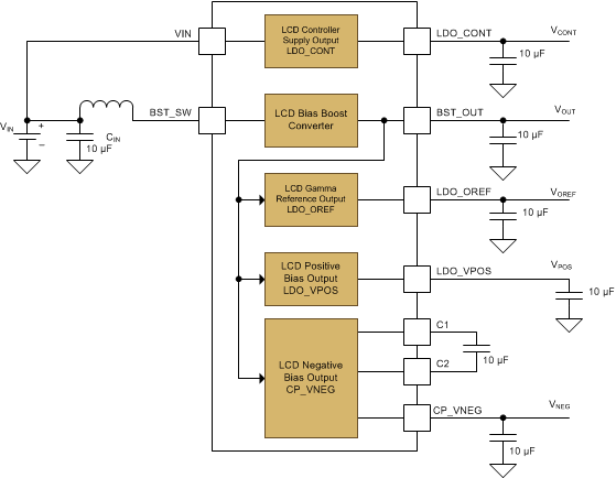 Figure 48. LCD Boost
8.3.4.2 Display Bias Power Sequencing (VPOS, VNEG, VOREF, VCONT)
The LM3631 supports configurable output power-up and power-down timing for VPOS, VNEG, VCONT and VOREF. The LED current sinks can start up after the bias voltages power ok signals (or after the timeout period has elapsed (20 ms typ.)) and shuts down before the bias power-down sequence begins. The bias power-down sequence does not start until after the LED current sinks have turned off.
The trigger for the power-up sequence is either a change from logic LOW to logic HIGH on the LCD_EN pin or the Display Bias Outputs bit. The trigger for the power-down sequence is either a change from logic HIGH to logic LOW on the LCD_EN pin or the Display Bias Outputs bit. The pull-downs or pull-ups for each output, if enabled, disengage immediately upon start-up of each respective output and re-engages immediately upon shutdown of each respective output.
Table 6. Start-Up and Shutdown Delays
| START-UP DELAY SETTING (LDO_OREF_SU_DLY, LDO_VPOS_SU_DLY, CP_VNEG_SU_DLY) (ms) | SHUTDOWN DELAY SETTING (LDO_OREF_SD_DLY, LDO_VPOS_SD_DLY, CP_VNEG_SD_DLY) (ms) |
|---|---|
| 0000 = 0 | 0000 = 0 |
| 0001 = 1 | 0001 = 1 |
| 0010 = 2 | 0010 = 2 |
| 0011 = 3 | 0011 = 3 |
| 0100 = 4 | 0100 = 4 |
| 0101 = 5 | 0101 = 5 |
| 0110 = 6 | 0110 = 6 |
| 0111 = 7 | 0111 = 7 |
| 1000 = 8 | 1000 = 8 |
| 1001 = 9 | 1001 = 9 |
| 1010 = 10 | 1010 = 10 |
| 1011 = 11 | 1011 = 11 |
| 1100 = 12 | 1100 = 12 |
| 1101 = 13 | 1101 = 13 |
| 1110 = 14 | 1110 = 14 |
| 1111 = 15 | 1111 = 15 |
LDO_CONT start-up/shutdown delay has a 3-bit programmable range.
Table 7. LDO_CONT Start-Up/Shutdown Delays
| LDO_CONT START-UP/SHUTDOWN DELAY SETTING (LDO_CONT_SU_DLY, LDO_CONT_SD_DLY) | START-UP/SHUTDOWN DELAY (ms) |
|---|---|
| 000 | 0 |
| 001 | 2 |
| 010 | 5 |
| 011 | 10 |
| 100 | 20 |
| 101 | 50 |
| 110 | 100 |
| 111 | 200 |
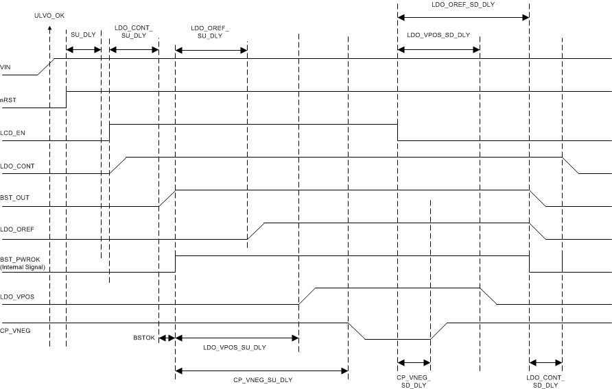 Figure 49. General LCD Bias Power Sequence Without Backlight
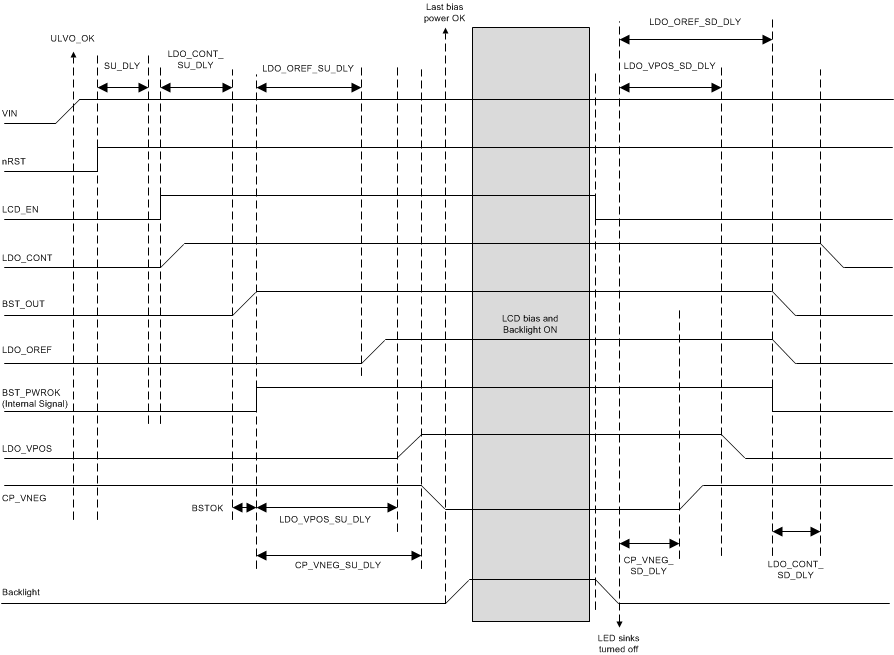 Figure 50. General LCD Bias Power Sequence With Backlight
8.3.4.2.1 Start-Up and Shutdown Delays
-
SU_DLY
Start-up delay from LCD_EN = HIGH to start up of the internal references, bias, and oscillator.
-
LDO_CONT_SU_DLY
Delay between the time LDO_CONT signal starts to rise ‘HIGH’, and the time before BST_OUT starts to rise. LDO_CONT delay can be adjusted with LDO_CONT_SU_DLY I2C register start-up delay bits. In case LDO_CONT is disabled, BST_OUT starts to rise after LCD_EN is set ‘HIGH’.
-
BSTOK
Bias boost startup delay. Time between the time when BST_OUT voltage starts to rise and the time when BST_PWROK (internal) signal rises to ‘HIGH’.
-
LDO_OREF_SU_DLY
Delay between the time when BST_PWROK signal rises to ‘HIGH’ and LDO_OREF signal starts to rise. Delay can be adjusted with I2C register start-up delay bits LDO_OREF_SU_DLY.
-
LDO_VPOS_SU_DLY
Delay between the time when BST_PWROK signal rises to ‘HIGH’ and LDO_VPOS signal starts to rise. Delay can be adjusted with I2C register start-up delay bits LDO_VPOS_SU_DLY.
-
CP_VNEG_SU_DLY
Delay between the time when BST_PWROK signal rises to ‘HIGH’ and CP_VNEG signal starts to fall. Delay can be adjusted with I2C register start-up delay bits CP_VNEG_SU_DLY. Note that there is a minimum delay of 500 µs (typ.) due to biasing of the flycap.
-
CP_VNEG_SD_DLY
Delay between the time when LCD_EN signal is set LOW and the time when CP_VNEG signal starts to rise. Delay can be adjusted with I2C register off delay bits CP_VNEG_SD_DLY.
-
LDO_VPOS_SD_DLY
Delay between the time when LCD_EN signal is set LOW and the time when LDO_VPOS signal starts to fall. Delay can be adjusted with I2C register off delay bits LDO_VPOS_SD_DLY.
-
LDO_OREF_SD_DLY
Delay between the time when LCD_EN signal is set LOW and the time when LDO_OREF signals start to fall. Delay can be adjusted with I2C register off delay bits LDO_OREF_SD_DLY.
-
LDO_CONT_SD_DLY
After last of the LDO_OREF, CP_VNEG, or LDO_VPOS shutdown time has ended LDO_CONT signal starts to fall in case it is enabled.
8.3.4.2.2 Special Conditions During Display Bias Power Sequencing
-
Short nRST Condition During Shutdown Sequence
If nRST is logic LOW for longer than the deglitch time, all appropriate outputs are sequenced down completely. If nRST is toggled or is held at logic HIGH before the all outputs are shutdown, the shutdown sequencing continues to turn off all outputs and set all the internal registers to the default state. Note that if nRST is toggled or is held at logic HIGH before all outputs are shut down, and FLAG pin is configured as fault, there are small glitches in the FLAG line after nRST is set HIGH.
-
Thermal Fault During Shutdown Sequence
A thermal fault, when the die temperature is greater than TSD, shuts down all outputs. When the die temperature drops by TSD(HYSTERESIS), the outputs can be re-started by toggling LCD_EN or the “LCD_EN” bit of register 0x00.
-
Backlight Sequence During LCD Bias Start-up Sequence
Backlight cannot be enabled before LCD bias start-up sequence is complete. If the backlight is enabled (via either the PWM or I2C register) before the LCD bias start-up sequence is complete, the backlight start-up sequence starts after LCD bias start-up sequence is complete.
8.3.4.3 Active Discharge
An active discharge is implemented for each output rail (LDO_OREF, LDO_VPOS, LDO_CONT and CP_VNEG) with internal switch resistance. The discharge function is programmable by I2C interface and is triggered by LCD_EN = “LOW”. During power-up, each output programmed to be actively discharged (at power-down) is actively discharged as long as it is not enabled internally.
8.3.4.4 LCD Bias Protection
The LM3631 provides OVP that monitors the LCD Bias boost output voltage (VOUT) and protects BST_OUT and BST_SW from exceeding safe operating voltages. The OVP threshold can be set with the I2C register bits. If there is an LCD bias overvoltage fault, an LCD_OVPFLT fault is set. The fault is cleared with the rising edge of LCD_EN or an I2C write '1' to the LCD_OVPFLT bit.
LDO_VPOS has an OCP that limits the maximum current drawn to 200 mA (typ.). If the fault condition persists over 2 ms, the LCD is shut down according to the normal shutdown sequence, and an LDO_VPOS_FLT fault is set. The fault must be cleared to enable power; the fault is cleared with rising edge of LCD_EN or an I2C write '1' to LDO_VPOS_FLT bit.
LDO_OREF has OCP that limits the maximum current drawn to 80 mA (typ.). If the fault condition persists over 2 ms, the LCD is shut down according to the normal shutdown sequence, and an LDO_OREF_FLT fault is set. The fault must be cleared to enable powers; the fault is cleared with rising edge of LCD_EN or I2C write '1' to LDO_OREF_FLT bit.
CP_VNEG has a short-circuit and OVP feature, which monitors the charge-pump voltage.
- If the charge-pump voltage goes 250 mv (typ.) below its target set-point, the charge pump is shut down. If the OVP persists for 2 ms, all bias outputs are turned off following the normal shutdown sequence, and a NEG_CP_OVP fault is set. The fault must be cleared, to re-enable the outputs, with the rising edge of LCD_EN or an I2C write '1' to NEG_CP_OVP bit.
- If the charge-pump voltage goes over –1 V, the charge pump is shut down, and a NEG_CP_SC fault gets set. The fault must be cleared, to re-enable the outputs, with rising edge of LCD_EN or an I2C write '1' to NEG_CP_SC.
8.3.5 Display Controller Power (VLDO_CONT)
The LM3631 supports an additional regulated output VLDO_CONT which can supply, for example, the display’s controller voltage. The LDO_CONT has a 2-bit programmable range with 1.8-V, 2.3-V, 2.8-V and 3.3-V values and can supply up to 80 mA. This LDO is powered directly from VIN voltage.
NOTE
When the LDO voltage is set to 2.8 V, VIN voltage must be kept over 2.8 V to ensure LDO proper functionality. Similarly, when LDO voltage is set to 3.3 V, the battery voltage must be kept over 3.3 V to ensure LDO proper functionality.
LDO_CONT has an OCP feature. If the OCP fault condition persists over 2 ms, a fault is set. LDO_CONT limits the current. Fault is cleared with rising edge of LCD_EN or an I2C write '1' to the LDO_CONT_FLT bit.
8.3.6 RESET Register
I2C register 0x14 is the register reset. Writing FFh into this register resets all I2C register values to default values. Default values are described in Table 1.
8.3.7 nRST Input
The nRST input is a global hardware enable for the LM3631. This pin must be pulled to logic HIGH to enable the device and the I2C-compatible interface. This pin is high-impedance and cannot be left floating. When this pin is at logic LOW, the LM3631 is placed in shutdown, the I2C-compatible interface is disabled, and the internal registers are reset to their default state. It is recommended that VIN has risen above a 2.7-V before setting nRST HIGH.
8.3.8 FLAG Pin
The FLAG pin can be used as an indicator to the application processor when the LM3631 encounters, for example, OVP. The fault conditions which set the FLAG pin to pull low can be programmed via I2C. Additionally, the power-good flag can be set to trigger from the flag for the bias voltages.
The FLAG pin is an open-drain output. When this pin is used, a pullup resistor is needed. If not used, this pin can be left floating.
Table 8. FLAG Pin Configuration
| FLAG PIN CONFIGURATION BITS | FLAG PIN INFORMATION |
|---|---|
| 00 | Flag disabled, no flag indication |
| 01 | Power-Good state, selectable with Power-Good flag control bits (PG_FLAG_CTRL) |
| 10 | Backlight on state |
| 11 | Fault state |
8.3.9 Power-Good Flag
The Power-Good flag can be used to indicate an application processor power-good situation of the bias voltages. The Power-Good flag information can be selected with Power-Good Flag control bits (PG_FLAG_CTRL). This information can be directed to the FLAG pin with FLAG pin configuration bits.
NOTE
When nRST is pulled low before the power sequence is complete, the Power-Good Flag indication is triggered even though the condition (described in Table 9) to trigger that the Power-Good flag is not fulfilled. When the Power-Good configuration is '00' (after last supply reaches target), LDO_VPOS, CP_VNEG, and LDO_OREF all need to be enabled.
Table 9. Power-Good Flag Configuration
| POWER-GOOD FLAG CONFIGURATION BITS | FLAG PIN INFORMATION DURING START-UP | FLAG PIN INFORMATION DURING SHUTDOWN |
|---|---|---|
| 00 | Power-Good bit set to '1' after last supply reaches target | Power-Good bit set to '0' after first supply falls below target |
| 01 | Power-Good bit set to '1' after LDO_VPOS reaches target | Power-Good bit set to '0' after LDO_VPOS falls below target |
| 10 | Power-Good bit set to '1' after CP_VNEG reaches target | Power-Good bit set to '0' after CP_VNEG falls below target |
| 11 | Power-Good bit set to '1' after LDO_OREF reaches target | Power-Good bit set to '0' after LDO_OREF falls below target |
8.3.10 OTP_SEL Pin
The OTP selection pin is dedicated for selection between two different default setups. Setting this pin to VBATT or GND selects the OTP from where the default setup is loaded. Note that this selection applies only for the backlight and LCD configuration registers (registers from 0x05h to 0x12h).
8.3.11 Thermal Shutdown
The LM3631 has Thermal Shutdown protection which shuts down the backlight, all bias voltage outputs and enters standby mode when the die temperature reaches or exceeds 140°C (typ.). When the die temperature falls below 120°C (typ.), the LM3631 comes out of standby. The I2C interface remains active during a Thermal Shutdown event. If a TSD fault occurs, TMPFLT fault is set — the fault is cleared by an I2C write '1' to TMPFLT bit or by setting LCD_EN high.
8.3.12 Undervoltage Lockout
The LM3631 has an undervoltage lockout feature (UVLO), which indicates of the device operation at low input voltages. If the supply voltage VIN is below the UVLO threshold, a UVLO fault is set. UVLO fault is cleared by an I2C write '1' to UVLO bit. UVLO does not shut down the outputs.
UVLO rising threshold is 2.6 V (typ.), and UVLO falling threshold is 2.5 V (typ.).
8.4 Device Functional Modes
8.4.1 Modes of Operation
-
Shutdown:
The LM3631 is in shutdown when nRST pin is low.
-
Standby:
After nRST pin is set high, and VIN is over UVLO limit, the LM3631 goes into Standby mode. Before entering Standby mode, references and bias currents are enabled (bias delay typically 200 µs), and registers are read from OTP (EPROM read delay typically 700 µs). In Standby mode references and bias currents are enabled, and I2C writes are allowed. LCD powers, and backlight are disabled.
-
Normal mode:
- LDO_CONT start-up: LDO_CONT is enabled. Programmable delay of 0 to 200 ms.
- LCD Boost start-up: LCD Boost is enabled. Waits until Boost output voltage is reached 90% of target value.
- LCD bias start-up enables, sequentially, LDO_VPOS, CP_VNEG, and LDO_OREF according to start-up delay settings.
When LCD_EN is set to high (pin or bit), the start-up sequence is started. During the start-up sequence LDO_CONT, LCD Boost, and LCD bias powers are started. If the LDO_CONT is disabled, the start-up sequence goes directly to LCD Boost start-up.
After the LCD bias start-up has completed, the LM3631 enters backlight start-up mode if BL_EN bit is set to ‘1’, and the PWM brightness value is different than 0. Even if the backlight is not enabled, LCD powers remains active. If the backlight is enabled, and BL_EN bit is set to ‘0’ or PWM brightness value is set to 0, backlight is disabled. LCD powers remains active.
If LCD_EN is set to ‘0’, the LM3631 shuts down backlight and bias powers and enters Standby mode. During power down the backlight is shut down first if it was enabled. After backlight shutdown is completed, the device enters LCD Bias shutdown. In LCD bias shutdown LDO_VPOS, CP_VNEG, and LDO_OREF are shut down sequentially according to shutdown delay settings. After the LDO_VPOS, CP_VNEG, and LDO_OREF shutdown sequence is complete, LCD Boost and LDO_CONT (if it was enabled) are shut down. LDO_CONT is shut down after adjustable delay (0 to 200 ms). Once LDO_CONT has shut down, the LM3631 enters Standby mode.
In a fault situation (thermal, backlight boost short circuit, LDO_OREF overcurrent, VPOS overcurrent, or CP short circuit), the device starts the shutdown sequence and enters Standby mode.
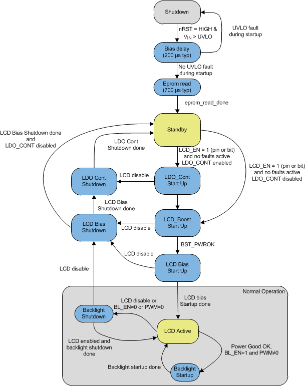 Figure 51. Modes of Operations
8.5 Programming
8.5.1 I2C-Compatible Serial Bus Interface
8.5.1.1 Interface Bus Overview
The I2C-compatible synchronous serial interface provides access to the programmable functions and registers on the device. This protocol uses a two-wire interface for bidirectional communications between the IC's connected to the bus. The two interface lines are the Serial Data Line (SDA) and the Serial Clock Line (SCL). These lines should be connected to a positive supply via a pull-up resistor and remain HIGH even when the bus is idle.
Every device on the bus is assigned a unique address and acts as either a Master or a Slave, depending whether it generates or receives the serial clock (SCL).
8.5.1.2 Data Transactions
One data bit is transferred during each clock pulse. Data is sampled during the high state of the serial clock (SCL). Consequently, throughout the clock’s high period, the data should remain stable. Any changes on the SDA line during the high state of the SCL and in the middle of a transaction, aborts the current transaction. New data should be sent during the low SCL state. This protocol permits a single data line to transfer both command/control information and data using the synchronous serial clock.
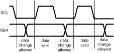 Figure 52. Data Validity
Each data transaction is composed of a Start Condition, a number of byte transfers (set by the software), and a Stop Condition to terminate the transaction. Every byte written to the SDA bus must be 8 bits long and is transferred with the most significant bit first. After each byte, an Acknowledge signal must follow. The following sections provide further details of this process.
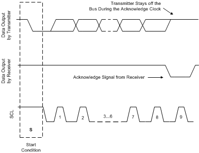 Figure 53. Acknowledge Signal
The Master device on the bus always generates the Start and Stop Conditions (control codes). After a Start Condition is generated, the bus is considered busy, and it retains this status until a certain time after a Stop Condition is generated. A high-to-low transition of the data line (SDA) while the clock (SCL) is high indicates a Start Condition. A low-to-high transition of the SDA line while the SCL is high indicates a Stop Condition.
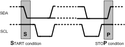 Figure 54. Start and Stop Conditions
In addition to the first Start Condition, a repeated Start Condition can be generated in the middle of a transaction. This allows another device to be accessed, or a register read cycle.
8.5.1.3 Acknowledge Cycle
The Acknowledge Cycle consists of two signals: the acknowledge clock pulse the master sends with each byte transferred, and the acknowledge signal sent by the receiving device.
The master generates the acknowledge clock pulse on the ninth clock pulse of the byte transfer. The transmitter releases the SDA line (permits it to go high) to allow the receiver to send the acknowledge signal. The receiver must pull down the SDA line during the acknowledge clock pulse and ensure that SDA remains low during the high period of the clock pulse, thus signaling the correct reception of the last data byte and its readiness to receive the next byte.
8.5.1.4 Acknowledge After Every Byte Rule
The master generates an acknowledge clock pulse after each byte transfer. The receiver sends an acknowledge signal after every byte received.
There is one exception to the “acknowledge after every byte” rule. When the master is the receiver, it must indicate to the transmitter an end of data by not-acknowledging (“negative acknowledge”) the last byte clocked out of the slave. This “negative acknowledge” still includes the acknowledge clock pulse (generated by the master), but the SDA line is not pulled down.
8.5.1.5 Addressing Transfer Formats
Each device on the bus has a unique slave address. The LM3631 operates as a slave device with the 7-bit address. If an 8-bit address is used for programming, the 8th bit is '1' for read and '0' for write. The 7-bit address for the LM3631 is 0x29.
Before any data is transmitted, the master transmits the address of the slave being addressed. The slave device should send an acknowledge signal on the SDA line, once it recognizes its address. The slave address is the first seven bits after a Start Condition. The direction of the data transfer (R/W) depends on the bit sent after the slave address — the eighth bit.
When the slave address is sent, each device in the system compares this slave address with its own. If there is a match, the device considers itself addressed and sends an acknowledge signal. Depending upon the state of the R/W bit (1:read, 0:write), the device acts as a transmitter or a receiver.
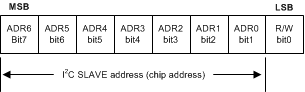 Figure 55. I2C Device Address
- Master device generates start condition.
- Master device sends slave address (7 bits) and the data direction bit (r/w = 0).
- Slave device sends acknowledge signal if the slave address is correct.
- Master sends control register address (8 bits).
- Slave sends acknowledge signal.
- Master sends data byte to be written to the addressed register.
- Slave sends acknowledge signal.
- If master sends further data bytes the control register address is incremented by one after acknowledge signal.
- Write cycle ends when the master creates stop condition.
Control Register Write Cycle
- Master device generates a start condition.
- Master device sends slave address (7 bits) and the data direction bit (r/w = 0).
- Slave device sends acknowledge signal if the slave address is correct.
- Master sends control register address (8 bits).
- Slave sends acknowledge signal
- Master device generates repeated start condition.
- Master sends the slave address (7 bits) and the data direction bit (r/w = 1).
- Slave sends acknowledge signal if the slave address is correct.
- Slave sends data byte from addressed register.
- If the master device sends acknowledge signal, the control register address is incremented by one. Slave device sends data byte from addressed register.
- Read cycle ends when the master does not generate acknowledge signal after data byte and generates stop condition.
Control Register Read Cycle
Table 10. I2C Data Read/Write(1)
| ADDRESS MODE | |
|---|---|
| Data Read | <Start Condition> <Slave Address><r/w =0>[Ack] <Register Addr>[Ack] <Repeated Start Condition> <Slave Address><r/w = 1>[Ack] [Register Data]<Ack or NAck> ...additional reads from subsequent register address possible <Stop Condition> |
| Data Write | <Start Condition> <Slave Address><r/w = 0>[Ack] <Register Addr>[Ack] <Register Data>[Ack] ...additional writes to subsequent register address possible <Stop Condition> |
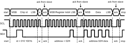 Figure 56. Register Write Format
When a READ function is to be accomplished, a WRITE function must precede the READ function, as show in the Read Cycle waveform.
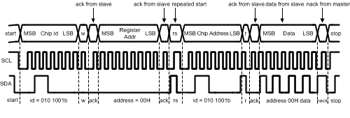 Figure 57. Register Read Format
NOTE
w = write (SDA = 0), r = read (SDA = 1), ack = acknowledge (SDA pulled down by either master or slave), rs = repeated start id = 7-bit chip address
8.6 Register Maps
Table 11. Device Control Register (0x00)
| [Bit 7] | [Bit 6] | [Bit 5] | [Bit 4] | [Bit 3] | [Bit 2] | [Bit 1] LCD_EN |
[Bit 0] BL_EN |
|---|---|---|---|---|---|---|---|
| Not Used | Not Used | Not Used | Not Used | Not Used | Not Used | 0 = LCD disabled 1 = LCD enabled |
0 = Backlight disabled 1 = Backlight enabled |
Table 12. LED Brightness Register LSB (0x01)
| [Bit 7] | [Bit 6] | [Bit 5] | [Bit 4] | [Bit 3] | [Bits 2:0] Brightness LSB |
||
|---|---|---|---|---|---|---|---|
| Not Used | Not Used | Not Used | Not Used | Not Used | BRT[2:0]. Lower 3 bits (LSB's) of brightness code. Concatenated with brightness bits in Register 0x02 (MSB). | ||
Table 13. LED Brightness Register MSB (0x02)
| [Bits 7:0] Brightness MSB | |||||||
|---|---|---|---|---|---|---|---|
| BRT[10:3]. Upper 8 bits (MSB's) of brightness code. Concatenated with brightness bits in Register 0x01 (LSB). |
Table 14. Faults Register (0x03)
| [Bit 7] BL_SCFLT |
[Bit 6] TMPFLT |
[Bit 5] BL_OCPFLT |
[Bit 4] BL_OVPFLT |
[Bit 3] LCD_OVPFLT |
[Bit 2] LDO_OREF_FLT |
[Bit 1] LDO_VPOS_FLT |
[Bit 0] UVLO FLAG |
|---|---|---|---|---|---|---|---|
| 0 = normal 1 = backlight short circuit condition |
0 = normal 1 = device has hit thermal shutdown threshold |
0 = normal 1 = fault, backlight boost current limit reached |
0 = normal 1 = fault, backlight boost overvoltage protection limit reached |
0 = normal 1 = fault, LCD boost overvoltage protection limit reached |
0 = normal 1 = fault, LDO_OREF short circuit condition |
0 = normal 1 = fault, LDO_VPOS short circuit condition |
0 = normal 1 = UVLO event |
Table 15. Faults and Power-Good Register (0x04)
| [Bit 7] | [Bit 6] | [Bit 5] | [Bit 4] | [Bit 3] NEG_CP_SC |
[Bit 2] NEG_CP_OVP |
[Bit 1] LDO_CONT_FLT |
[Bit 0] PG_FLAG |
|---|---|---|---|---|---|---|---|
| Not Used | Not Used | Not Used | Not Used | 0 = normal 1 = fault, negative chargepump short circuit condition |
0 = normal 1 = fault, negative chargepump overvoltage protection limit reached |
0 = normal 1 = fault, LDO Controller current limit reached |
Power-Good flag |
Table 16. Backlight Configuration (Auto Frequency Threshold) Register 1 (0x05)
| [Bits 7:0] AUTO_FREQ_THRES |
|||||||
|---|---|---|---|---|---|---|---|
LED current threshold value. When the Auto Frequency Select Mode Bit is ‘1’ (Bit[3] in register 0x07), the 8 bit code in this register (AUTOFREQ_THRESH) is compared against the MSB’s of the I2C Brightness code (BRT [10:3]), and this comparison is used to determine whether the device operates in Low Frequency or High Frequency Mode.
|
Table 17. Backlight Configuration Register 2 (0x06)
| [Bit 7] | [Bit 6] | [Bit 5] LINEAR_MAPPER |
[Bit 4] | [Bit 3] STRING_MODE |
[Bit 2] INDUCTOR |
[Bits 1:0] PEAK_CURR_LIM |
|
|---|---|---|---|---|---|---|---|
| Not Used | Not Used | 0= Exponential mapping in use 1 = Linear mapping in use |
Not Used | 0 = Both LED strings enabled 1 = Only LED string 1 enabled |
0 = Inductor typical value = 22 µH 1 = Inductor typical value = 10 µH |
00 = 600 mA 01 = 700 mA 10 = 800 mA 11 = 900 mA |
|
Table 18. Backlight Configuration Register 3 (0x07)
| [Bits 7:6] SEL_I |
[Bits 5:4] SEL_P |
[Bit 3] BL_AUTOFRQ |
[Bits 2:1] BL_BST_OVP |
[Bit 0] BL_BST_FREQ |
|||
|---|---|---|---|---|---|---|---|
| Backlight boost compensator adjustment. Select value according to number of LEDs in LED string. | Backlight boost compensator adjustment. Select value according to inductor | 0 = Manual frequency mode 1 = Auto frequency mode |
Backlight Boost OVP target 00 = 17 V 01 = 21 V 10 = 25 V 11 = 29 V |
Backlight Boost frequency 0 = 500 kHz 1 = 1 MHz |
|||
Table 19. Backlight Configuration Register 4 (0x08)
| [Bit 7] PWM_EDGE_DET_SEL |
[Bit 6] PWM POLARITY |
[Bits 5:4] HYSTERESIS |
[Bits 3:2] BRT_MODE |
[Bit 1] EN__ADV_SLOPE |
[Bit 0] DISABLE_DITHER |
||
|---|---|---|---|---|---|---|---|
| PWM edge detection selection 0 = PWM measured from rising edge 1 = PWM measured from falling edge |
0 = PWM active polarity LOW 1 = PWM active polarity HIGH |
PWM input hysteresis selection (change in 11-bit brightness) 00 = 0.05% shift causes change 01 = 0.1% shift causes change 10 = 0.2% shift causes change 11 = 0.4% shift causes change |
Brightness mode selection 00 = I2C register used for brightness control 01 = PWM input duty cycle used for brightness control 10 = I2C code multiplied with PWM duty cycle before sloping 11 = Sloped I2C brightness code multiplied with PWM duty cycle |
0 = Advanced slope disabled 1 = Advanced slope enabled |
0 = Dither enabled 1 = Dither disabled |
||
Table 20. Backlight Configuration Register 5 (0x09)
| [Bits 7:4] SLOPE |
[Bits 3:0] DITHER_FREQ_SEL |
||||||
|---|---|---|---|---|---|---|---|
| 0000 = Slope function disabled, immediate brightness change 0001 = 1 ms 0010 = 2 ms 0011 = 5 ms 0100 = 10 ms 0101 = 20 ms 0110 = 50 ms 0111 = 100 ms 1000 = 250 ms 1001 = 500 ms 1010 = 750 ms 1011 = 1000 ms 1100 = 1500 ms 1101 = 2000 ms 1110 = 3000 ms 1111 = 4000 ms |
Dithering frequency selection 0000 = 62.5 kHz 0001 = 31.3 kHz 0010 = 15.6 kHz 0011 = 7.8 kHz 0100 = 3.9 kHz 0101 = 1.95 kHz 0110 = 977 Hz 0111 = 488 Hz 1000 = 244 Hz 1001 = 122 Hz |
Table 21. LCD Configuration Register 1 (0x0A)
| [Bit 7] | [Bit 6] LDO_CONT_SD_PULLDN |
[Bit 5] LDO_OREF_SD_PULLDN |
[Bit 4] CP_VNEG_SD_PULLUP |
[Bit 3] LDO_VPOS_SD_PULLDN |
[Bit 2] LDO_VPOS_EN |
[Bit 1] CP_VNEG_EN |
[Bit 0] LDO_OREF_EN |
|---|---|---|---|---|---|---|---|
| Not Used | 0 = LDO_CONT pull-down resistor disabled 1 = LDO_CONT pull-down resistor enabled |
0 = LDO_OREF pull-down resistor disabled 1 = LDO_OREF pull-down resistor enabled |
0 = CP_VNEG pull-up resistor disabled 1 = CP_VNEG pull-up resistor enabled |
0 = LDO_VPOS pull-down resistor disabled 1 = LDO_VPOS pull-down resistor enabled |
0 = LDO_VPOS disabled 1 = LDO_VPOS enabled |
0 = CP_VNEG disabled 1 = CP_VNEG enabled |
0 = LDO_OREF disabled 1 = LDO_OREF enabled |
Table 22. LCD Configuration Register 2 (LDO_CONT) (0x0B)
| [Bit 7] | [Bits 6:4] LDO_CONT_SU_DELAY |
[Bits 3:1] LDO_CONT_SD_DELAY |
[Bit 0] LDO_CONT_EN |
||||
|---|---|---|---|---|---|---|---|
| Not Used | LDO_CONT start-up delay 000 = 0 ms 001 = 2 ms 010 = 5 ms 011 = 10 ms 100 = 20 ms 101 = 50 ms 110 = 100 ms 111 = 200 ms |
LDO_CONT shutdown delay 000 = 0 ms 001 = 2 ms 010 = 5 ms 011 = 10 ms 100 = 20 ms 101 = 50 ms 110 = 100 ms 111 = 200 ms |
0 = LDO_CONT disabled 1 = LDO_CONT enabled |
||||
Table 23. LCD Configuration Register 3 (0x0C)
| [Bits 7:6] LDO_CONT_VOUT |
[Bits 5:0] LCD_BST_OUT |
||||||
|---|---|---|---|---|---|---|---|
| LDO_CONT output voltage 00 = 1.8 V 01 = 2.3 V 10 = 2.8 V 11 = 3.3 V |
LCD Boost output voltage 000 000 = 4.50 V 000 001 = 4.55 V 000 010 = 4.60 V 000 011 = 4.65 V 000 100 = 4.70 V ... 010 111 = 5.65 V 011 000 = 5.70 V 011 001 = 5.75 V ... 100 001 = 6.15 V 100 010 = 6.20 V 100 011 = 6.25 V 100 100 = 6.30 V 100 101 = 6.35 V |
||||||
Table 24. LCD Configuration Register 4 (LDO_VPOS) (0x0D)
| [Bit 7] | [Bit 6] | [Bits 5:0] LDO_VPOS_TARGET |
|||||
|---|---|---|---|---|---|---|---|
| Not Used | Not Used | 000 000 = 4.00 V 000 001 = 4.05 V 000 010 = 4.10 V 000 011 = 4.15 V 000 100 = 4.20 V ... 011 011 = 5.35 V 011 100 = 5.40 V 011 101 = 5.45 V ... 100 100 = 5.80 V 100 101 = 5.85 V 100 110 = 5.90 V 100 111 = 5.95 V 101 000 = 6.00 V (6.00V is the maximum level regardless of the adjustment level above value '101 000') |
|||||
Table 25. LCD Configuration Register 5 (CP_VNEG) (0x0E)
| [Bit 7] | [Bit 6] | [Bits 5:0] CP_VNEG_TARGET |
|||||
|---|---|---|---|---|---|---|---|
| Not Used | Not Used | 000 000 = –4.00 V 000 001 = –4.05 V 000 010 = –4.10 V 000 011 = –4.15 V 000 100 = –4.20 V ... 011 011 = –5.35 V 011 100 = –5.40 V 011 101 = –5.45 V ... 100 100 = –5.80 V 100 101 = –5.85 V 100 110 = –5.90 V 100 111 = –5.95 V 101 000 = –6.00 V (–6.00V is the maximum level regardless of the adjustment level above value '101 000') |
|||||
Table 26. LCD Configuration Register 6 (LDO_OREF) (0x0F)
| [Bit 7] | [Bit 6] | [Bits 5:0] LDO_OREF_TARGET |
|||||
|---|---|---|---|---|---|---|---|
| Not Used | Not Used | 000 000 = 4.00 V 000 001 = 4.05 V 000 010 = 4.10 V 000 011 = 4.15 V 000 100 = 4.20 V ... 011 011 = 5.35 V 011 100 = 5.40 V 011 101 = 5.45 V ... 100 100 = 5.80 V 100 101 = 5.85 V 100 110 = 5.90 V 100 111 = 5.95 V 101 000 = 6.00 V (6.00V is the maximum level regardless of the adjustment level above value '101 000') |
|||||
Table 27. LCD Configuration Register 7 (LDO_VPOS Sequence Control) (0x10)
| [Bits 7:4] LDO_VPOS START-UP DELAY |
[Bits 3:0] LDO_VPOS SHUTDOWN DELAY |
||||||
|---|---|---|---|---|---|---|---|
| 0000 = 0.0 ms 0001 = 1.0 ms 0010 = 2.0 ms 0011 = 3.0 ms 0100 = 4.0 ms 0101 = 5.0 ms 0110 = 6.0 ms 0111 = 7.0 ms 1000 = 8.0 ms 1001 = 9.0 ms 1010 = 10.0 ms 1011 = 11.0 ms 1100 = 12.0 ms 1101 = 13.0 ms 1110 =14.0 ms 1111 = 15.0 ms |
0000 = 0.0 ms 0001 = 1.0 ms 0010 = 2.0 ms 0011 = 3.0 ms 0100 = 4.0 ms 0101 = 5.0 ms 0110 = 6.0 ms 0111 = 7.0 ms 1000 = 8.0 ms 1001 = 9.0 ms 1010 = 10.0 ms 1011 = 11.0 ms 1100 = 12.0 ms 1101 = 13.0 ms 1110 =14.0 ms 1111 = 15.0 ms |
Table 28. LCD Configuration Register 8 (CP_VNEG Sequence Control) (0x11)
| [Bits 7:4] CP_VNEG START-UP DELAY (ms) |
[Bits 3:0] CP_VNEG SHUTDOWN DELAY (ms) |
||||||
|---|---|---|---|---|---|---|---|
| 0000 = 0.0 ms 0001 = 1.0 ms 0010 = 2.0 ms 0011 = 3.0 ms 0100 = 4.0 ms 0101 = 5.0 ms 0110 = 6.0 ms 0111 = 7.0 ms 1000 = 8.0 ms 1001 = 9.0 ms 1010 = 10.0 ms 1011 = 11.0 ms 1100 = 12.0 ms 1101 = 13.0 ms 1110 =14.0 ms 1111 = 15.0 ms |
0000 = 0.0 ms 0001 = 1.0 ms 0010 = 2.0 ms 0011 = 3.0 ms 0100 = 4.0 ms 0101 = 5.0 ms 0110 = 6.0 ms 0111 = 7.0 ms 1000 = 8.0 ms 1001 = 9.0 ms 1010 = 10.0 ms 1011 = 11.0 ms 1100 = 12.0 ms 1101 = 13.0 ms 1110 =14.0 ms 1111 = 15.0 ms |
Table 29. LCD Configuration Register 9 (LDO_OREF Sequence Control) (0x12)
| [Bits 7:4] LDO_OREF START-UP DELAY |
[Bits 3:0] LDO_OREF SHUTDOWN DELAY |
||||||
|---|---|---|---|---|---|---|---|
| 0000 = 0.0 ms 0001 = 1.0 ms 0010 = 2.0 ms 0011 = 3.0 ms 0100 = 4.0 ms 0101 = 5.0 ms 0110 = 6.0 ms 0111 = 7.0 ms 1000 = 8.0 ms 1001 = 9.0 ms 1010 = 10.0 ms 1011 = 11.0 ms 1100 = 12.0 ms 1101 = 13.0 ms 1110 =14.0 ms 1111 = 15.0 ms |
0000 = 0.0 ms 0001 = 1.0 ms 0010 = 2.0 ms 0011 = 3.0 ms 0100 = 4.0 ms 0101 = 5.0 ms 0110 = 6.0 ms 0111 = 7.0 ms 1000 = 8.0 ms 1001 = 9.0 ms 1010 = 10.0 ms 1011 = 11.0 ms 1100 = 12.0 ms 1101 = 13.0 ms 1110 =14.0 ms 1111 = 15.0 ms |
Table 30. FLAG Configuration Register (0x13)
| [Bit 7] | [Bit 6] | [Bit 5] | [Bit 4] FLAG_PIN_POLARITY |
[Bits 3:2] PG_FLAG_CTRL |
[Bits 1:0] PG_FLAG_CONFIG |
||
|---|---|---|---|---|---|---|---|
| Not Used | Not Used | Not Used | 0 =FLAG pin active polarity LOW 1 = FLAG pin active polarity HIGH |
00 = Power-Good set after last supply reaches target 01 = Power-Good set after LDO_VPOS 10 = Power-Good set after CP_VNEG 11 = Power-Good set after LDO_OREF |
00 = FLAG disabled, no flag indication 01 = Power-Good state, selectable with PG_FLAG_CTRL bits 10 = Backlight ON state 11 = Fault state |
||
Table 31. BOOT/RESET Register (0x14)
| [Bit 7:0] BOOT |
|||||||
|---|---|---|---|---|---|---|---|
| Write FFh to set all I2C registers to RESET value |
Table 32. Revision Register (0x16)
| [Bit 7:6] DIE TRACEABILITY |
[Bit 5:3] OTP REVISION |
[Bit 2:0] DEVICE REVISION |
|||||
|---|---|---|---|---|---|---|---|
| Die Traceability Information | Device OTP Revision Information | Device Revision Information | |||||