SNVS834 August 2014 LM3631
PRODUCTION DATA.
- 1 Features
- 2 Applications
- 3 Description
- 4 Revision History
- 5 Device Comparison Table
- 6 Pin Configuration and Functions
- 7 Specifications
-
8 Detailed Description
- 8.1 Overview
- 8.2 Functional Block Diagram
- 8.3 Features Description
- 8.4 Device Functional Modes
- 8.5 Programming
- 8.6 Register Maps
- 9 Application and Implementation
- 10Power Supply Recommendations
- 11Layout
- 12Device and Documentation Support
- 13Mechanical, Packaging, and Orderable Information
Package Options
Mechanical Data (Package|Pins)
- YFF|24
Thermal pad, mechanical data (Package|Pins)
Orderable Information
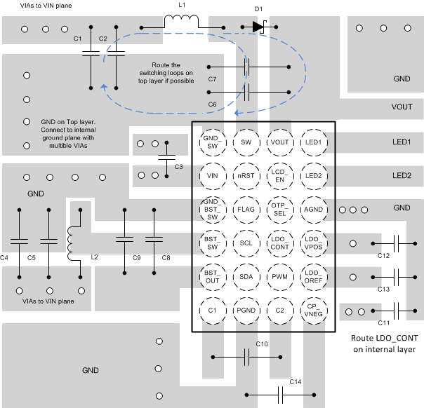
11 Layout
11.1 Layout Guidelines
- Place the boost converters output capacitors as close to the output voltage and GND pins as possible.
- Minimize the boost converter switching loops by placing the input capacitors and inductors close to GND and switch pins.
- If possible, route the switching loops on top layer only. For best efficiency, try to minimize copper on the switch node to minimize switch pin parasitic capacitance while preserving adequate routing width.
- VIN input voltage pin needs to be bypassed to ground with a low-ESR bypass capacitor. Place the capacitor as close to VIN pin as possible
- Place the output capacitors of the LDOs as close to output pins as possible. Also place the charge pump flying capacitor and output capacitor close to respective pins.
- Route the internal pins on the second layer. Use offset micro vias to go from top layer to mid layer1. Avoid routing the signal traces directly under the switching loops of the boost converters.
11.2 Layout Example