SNVS967A August 2014 – November 2014 LM3643
PRODUCTION DATA.
- 1 Features
- 2 Applications
- 3 Description
- 4 Simplified Schematic
- 5 Revision History
- 6 Device Comparison Table
- 7 Pin Configuration and Functions
- 8 Specifications
-
9 Detailed Description
- 9.1 Overview
- 9.2 Functional Block Diagram
- 9.3 Feature Description
- 9.4 Device Functioning Modes
- 9.5 Programming
- 9.6
Register Descriptions
- 9.6.1 Enable Register (0x01)
- 9.6.2 IVFM Register (0x02)
- 9.6.3 LED1 Flash Brightness Register (0x03)
- 9.6.4 LED2 Flash Brightness Register (0x04)
- 9.6.5 LED1 Torch Brightness Register (0x05)
- 9.6.6 LED2 Torch Brightness Register (0x06)
- 9.6.7 Boost Configuration Register (0x07)
- 9.6.8 Timing Configuration Register (0x08)
- 9.6.9 TEMP Register (0x09)
- 9.6.10 Flags1 Register (0x0A)
- 9.6.11 Flags2 Register (0x0B)
- 9.6.12 Device ID Register (0x0C)
- 9.6.13 Last Flash Register (0x0D)
- 10Applications and Implementation
- 11Power Supply Recommendations
- 12Layout
- 13Device and Documentation Support
- 14Mechanical, Packaging, and Orderable Information
Package Options
Mechanical Data (Package|Pins)
- YFF|12
Thermal pad, mechanical data (Package|Pins)
Orderable Information
10 Applications and Implementation
NOTE
Information in the following applications sections is not part of the TI component specification, and TI does not warrant its accuracy or completeness. TI’s customers are responsible for determining suitability of components for their purposes. Customers should validate and test their design implementation to confirm system functionality.
10.1 Application Information
The LM3643 can drive two flash LEDs at currents up to 1.5 A per LED. The total LED current the LM3643 boost can deliver is 1.5 A (ILED1 + ILED2 ). The 2-MHz/4-MHz DC/DC boost regulator allows for the use of small value discrete external components.
10.2 Typical Application
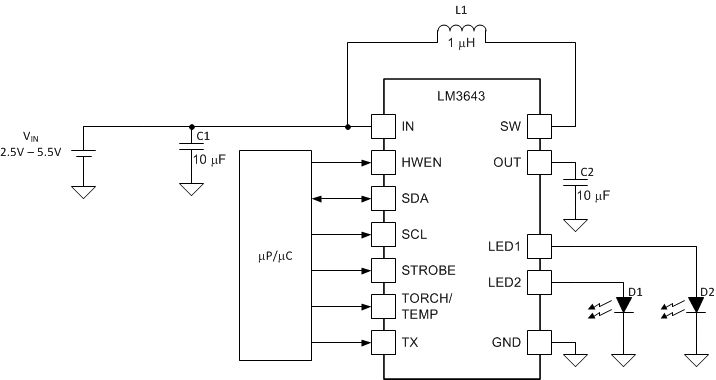 Figure 36. LM3643 Typical Application
10.2.1 Design Requirements
Example requirements based on default register values:
| DESIGN PARAMETER | EXAMPLE VALUE |
|---|---|
| Input Voltage Range | 2.5 V to 5.5 V |
| Brightness Control | I2C Register |
| LED Configuration | 2 Parallel Flash LEDs |
| Boost Switching Frequency | 2 MHz (4 MHz selectable) |
| Flash Brightness | 750 mA per LED |
10.2.2 Detailed Design Procedure
10.2.2.1 Output Capacitor Selection
The LM3643 is designed to operate with a 10-µF ceramic output capacitor. When the boost converter is running, the output capacitor supplies the load current during the boost converter on-time. When the NMOS switch turns off, the inductor energy is discharged through the internal PMOS switch, supplying power to the load and restoring charge to the output capacitor. This causes a sag in the output voltage during the on-time and a rise in the output voltage during the off-time. The output capacitor is therefore chosen to limit the output ripple to an acceptable level depending on load current and input/output voltage differentials and also to ensure the converter remains stable.
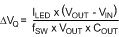
Larger capacitors such as a 22-µF or capacitors in parallel can be used if lower output voltage ripple is desired. To estimate the output voltage ripple considering the ripple due to capacitor discharge (ΔVQ) and the ripple due to the capacitors ESR (ΔVESR) use the following equations:
For continuous conduction mode, the output voltage ripple due to the capacitor discharge is:
The output voltage ripple due to the output capacitors ESR is found by:
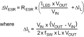
In ceramic capacitors the ESR is very low so the assumption is that 80% of the output voltage ripple is due to capacitor discharge and 20% from ESR. Table 1 lists different manufacturers for various output capacitors and their case sizes suitable for use with the LM3643.
10.2.2.2 Input Capacitor Selection
Choosing the correct size and type of input capacitor helps minimize the voltage ripple caused by the switching of the LM3643 boost converter and reduce noise on the boost converter's input pin that can feed through and disrupt internal analog signals. In the typical application circuit a 10-µF ceramic input capacitor works well. It is important to place the input capacitor as close as possible to the LM3643 input (IN) pin. This reduces the series resistance and inductance that can inject noise into the device due to the input switching currents. Table 1 lists various input capacitors recommended for use with the LM3643.
Table 1. Recommended Input/Output Capacitors (X5R/X7R Dielectric)
| MANUFACTURER | PART NUMBER | VALUE | CASE SIZE | VOLTAGE RATING |
|---|---|---|---|---|
| TDK Corporation | C1608JB0J106M | 10 µF | 0603 (1.6 mm × 0.8 mm × 0.8 mm) | 6.3 V |
| TDK Corporation | C2012JB1A106M | 10 µF | 0805 (2.0 mm × 1.25 mm × 1.25 mm) | 10 V |
| Murata | GRM188R60J106M | 10 µF | 0603 (1.6 mm x 0.8 mm x 0.8 mm) | 6.3 V |
| Murata | GRM21BR61A106KE19 | 10 µF | 0805 (2.0 mm × 1.25 mm × 1.25 mm) | 10 V |
10.2.2.3 Inductor Selection
The LM3643 is designed to use a 0.47-µH or 1-µH inductor. Table 2 lists various inductors and their manufacturers that work well with the LM3643. When the device is boosting (VOUT > VIN) the inductor is typically the largest area of efficiency loss in the circuit. Therefore, choosing an inductor with the lowest possible series resistance is important. Additionally, the saturation rating of the inductor should be greater than the maximum operating peak current of the LM3643. This prevents excess efficiency loss that can occur with inductors that operate in saturation. For proper inductor operation and circuit performance, ensure that the inductor saturation and the peak current limit setting of the LM3643 are greater than IPEAK in the following calculation:
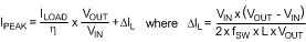
where
- ƒSW = 2 or 4 MHz
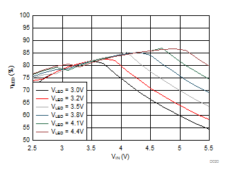
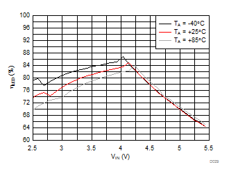
Efficiency details can be found in the Application Curves.
Table 2. Recommended Inductors
| MANUFACTURER | L | PART NUMBER | DIMENSIONS (L×W×H) | ISAT | RDC |
|---|---|---|---|---|---|
| TOKO | 0.47 µH | DFE201610P-R470M | 2.0 mm x 1.6 mm x 1.0 mm | 4.1 A | 32 mΩ |
| TOKO | 1 µH | DFE201610P-1R0M | 2.0 mm x 1.6 mm x 1.0 mm | 3.7 A | 58 mΩ |
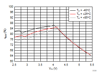
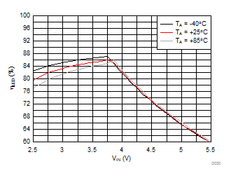
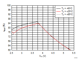
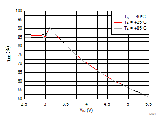
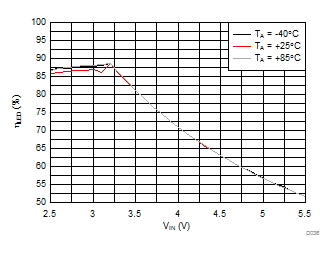
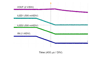
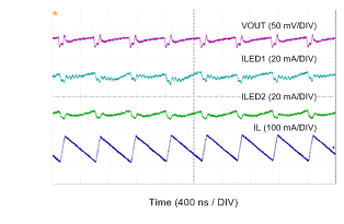
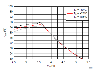
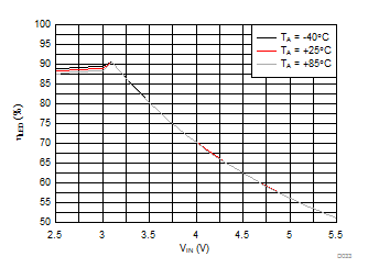
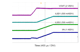
10.2.3 Application Curves
Ambient temperature is 25°C, input voltage is 3.6V, HWEN = VIN, CIN = 2 × 10 µF, COUT = 2 × 10 µF and L = 1 µH, unless otherwise noted.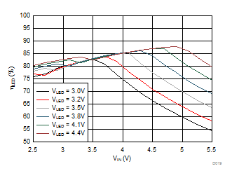
| ILED = 1.5 A | ƒSW = 2 MHz | Flash |
| ILED = 1.5A | ƒSW = 2 MHz | Flash |
| VLED = 3.55 V |
| ILED = 1 A | ƒSW = 2 MHz | Flash |
| VLED = 3.32 V |
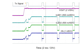
| ILED1 and LED2 = 729 mA | Flash | |
| VLED = 3.18 V | ƒSW = 2 MHz |
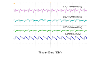
| ILED = 179 mA | ƒSW = 4 MHz | |
| VLED = 2.83 V | Torch |
| ILED1 and LED2 = 179 mA | ƒSW = 4 MHz | |
| VLED = 2.83 V | Torch |
| ILED1 = ILED2 = 730 mA | ƒSW = 2 MHz | |
| VLED = 3.18 V |
| ILED1 = ILED2 = 730 mA | ƒSW = 2 MHz | |
| VLED = 3.18 V |
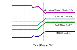
| ILED1 = ILED2 = 730 mA | ƒSW = 2 MHz | |
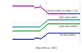
| VLED = 3.18 V | VIVFM = 3.2 V |
| ILED1 = ILED2 = 730 mA | ƒSW = 2 MHz | |||
| VLED = 3.18 V | VIVFM = 3.2 V |
| ILED = 1.5 A | ƒSW = 2 MHz | Flash |
| ILED = 1.5A | ƒSW = 4 MHz | Flash |
| VLED = 3.55 V |
| ILED = 729 mA | ƒSW = 2 MHz | Flash |
| VLED = 3.18 V |
| ILED = 179 mA | Torch | |
| VLED = 2.83 V | ƒSW = 2 MHz |
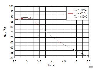
| ILED1 and LED2 = 179 mA | ƒSW = 2 MHz | |
| VLED = 2.83 V | Torch |
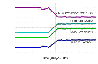
| ILED1 = ILED2 = 730 mA | ƒSW = 2 MHz | |
| VLED = 3.18 V |
| ILED1 = ILED2 = 730 mA | ƒSW = 2 MHz | |
| VLED = 3.18 V |
| ILED1 = ILED2 = 730 mA | ƒSW = 4 MHz | |
| VLED = 3.18 V |
| ILED1 = ILED2 = 730 mA | ƒSW = 2 MHz | |
| VLED = 3.18 V | VIVFM = 3.2 V |