SNVS967A August 2014 – November 2014 LM3643
PRODUCTION DATA.
- 1 Features
- 2 Applications
- 3 Description
- 4 Simplified Schematic
- 5 Revision History
- 6 Device Comparison Table
- 7 Pin Configuration and Functions
- 8 Specifications
-
9 Detailed Description
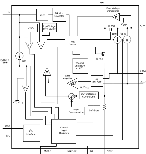
- 9.1 Overview
- 9.2 Functional Block Diagram
- 9.3 Feature Description
- 9.4 Device Functioning Modes
- 9.5 Programming
- 9.6
Register Descriptions
- 9.6.1 Enable Register (0x01)
- 9.6.2 IVFM Register (0x02)
- 9.6.3 LED1 Flash Brightness Register (0x03)
- 9.6.4 LED2 Flash Brightness Register (0x04)
- 9.6.5 LED1 Torch Brightness Register (0x05)
- 9.6.6 LED2 Torch Brightness Register (0x06)
- 9.6.7 Boost Configuration Register (0x07)
- 9.6.8 Timing Configuration Register (0x08)
- 9.6.9 TEMP Register (0x09)
- 9.6.10 Flags1 Register (0x0A)
- 9.6.11 Flags2 Register (0x0B)
- 9.6.12 Device ID Register (0x0C)
- 9.6.13 Last Flash Register (0x0D)
- 10Applications and Implementation
- 11Power Supply Recommendations
- 12Layout
- 13Device and Documentation Support
- 14Mechanical, Packaging, and Orderable Information
Package Options
Mechanical Data (Package|Pins)
- YFF|12
Thermal pad, mechanical data (Package|Pins)
Orderable Information
9 Detailed Description
9.1 Overview
The LM3643 is a high-power white LED flash driver capable of delivering up to 1.5 A in either of the two parallel LEDs. The total allowed LED current during operation of the LM3643 (ILED1+ILED2) is 1.5 A. The device incorporates a 2-MHz or 4-MHz constant frequency-synchronous current-mode PWM boost converter and dual high-side current sources to regulate the LED current over the 2.5-V to 5.5-V input voltage range.
The LM3643 PWM DC/DC boost converter switches and boosts the output to maintain at least VHR across each of the current sources (LED1/2). This minimum headroom voltage ensures that both current sources remain in regulation. If the input voltage is above the LED voltage + current source headroom voltage the device does not switch, but turns the PFET on continuously (Pass mode). In Pass mode the difference between (VIN − ILED x RPMOS) and the voltage across the LED is dropped across the current source.
The LM3643 has three logic inputs including a hardware Flash Enable (STROBE), a hardware Torch Enable (TORCH/TEMP, TORCH = default), and a Flash Interrupt input (TX) designed to interrupt the flash pulse during high battery-current conditions. These logic inputs have internal 300-kΩ (typ.) pulldown resistors to GND.
Additional features of the LM3643 include an internal comparator for LED thermal sensing via an external NTC thermistor and an input voltage monitor that can reduce the Flash current during low VIN conditions. It also has a Hardware Enable (HWEN) pin that can be used to reset the state of the device and the registers by pulling the HWEN pin to ground.
Control is done via an I2C-compatible interface. This includes adjustment of the Flash and Torch current levels, changing the Flash Timeout Duration, and changing the switch current limit. Additionally, there are flag and status bits that indicate flash current time-out, LED overtemperature condition, LED failure (open/short), device thermal shutdown, TX interrupt, and VIN undervoltage conditions.
9.2 Functional Block Diagram
9.3 Feature Description
9.3.1 Flash Mode
In Flash Mode, the LED current sources (LED1/2) provide 128 target current levels from 10.9 mA to 1500 mA. The total allowed LED current during operation is 1.5A (ILED1 + ILED2 = 1.5 A). Once the Flash sequence is activated the current source (LED) ramps up to the programmed Flash current by stepping through all current steps until the programmed current is reached. The headroom in the two current sources can be regulated to provide 10.9 mA to 1.5 A on each of the two output legs. There is an option in the register settings to keep the two currents in the output leg the same.
When the device is enabled in Flash Mode through the Enable Register, all mode bits in the Enable Register are cleared after a flash time-out event.
9.3.2 Torch Mode
In Torch mode, the LED current sources (LED1/2) provide 128 target current levels from 0.977 mA to 179 mA. The Torch currents are adjusted via the LED1 and LED2 LED Torch Brightness Registers. Torch mode is activated by the Enable Register (setting M1, M0 to '10'), or by pulling the TORCH/TEMP pin HIGH when the pin is enabled (Enable Register) and set to Torch Mode. Once the TORCH sequence is activated the active current sources (LED1/2) ramps up to the programmed Torch current by stepping through all current steps until the programmed current is reached. The rate at which the current ramps is determined by the value chosen in the Timing Register.
Torch Mode is not affected by Flash Timeout or by a TX Interrupt event.
9.3.3 IR Mode
In IR Mode, the target LED current is equal to the value stored in the LED1/2 Flash Brightness Registers. When IR mode is enabled (setting M1, M0 to '01'), the boost converter turns on and set the output equal to the input (pass-mode). At this point, toggling the STROBE pin enables and disables the LED1/2 current sources (if enabled). The strobe pin can only be set to be Level sensitive, meaning all timing of the IR pulse is externally controlled. In IR Mode, the current sources do not ramp the LED outputs to the target. The current transitions immediately from off to on and then on to off.
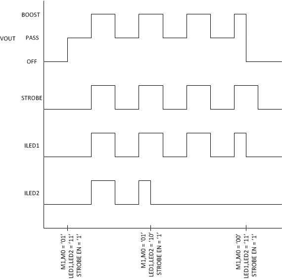 Figure 27. IR Mode with Boost
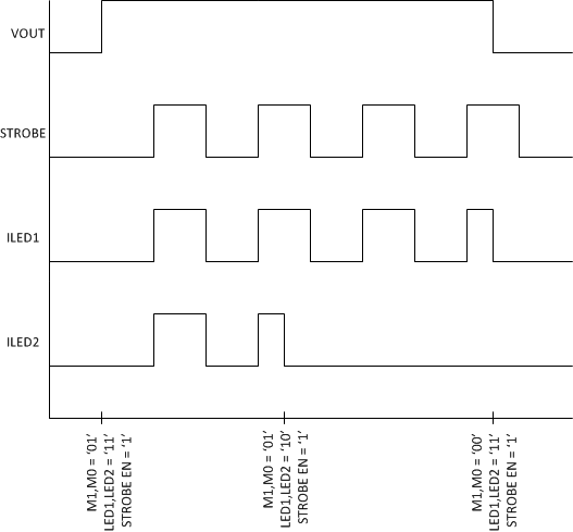 Figure 28. IR Mode Pass Only
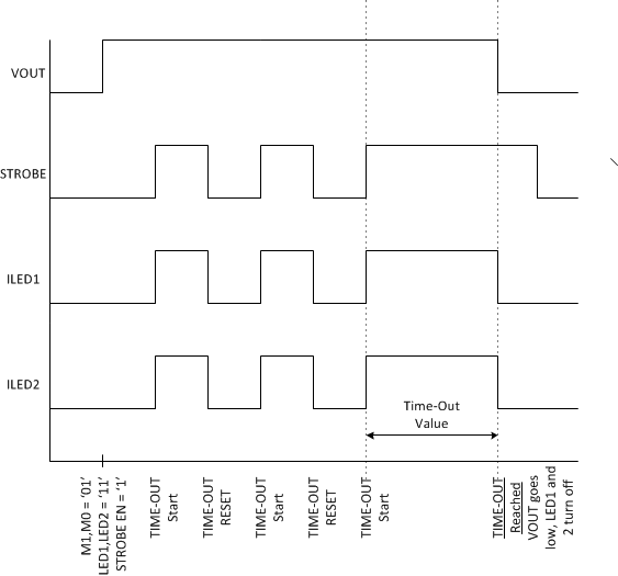 Figure 29. IR Mode Timeout
9.4 Device Functioning Modes
9.4.1 Start-Up (Enabling The Device)
Turn on of the LM3643 Torch and Flash modes can be done through the Enable Register. On start-up, when VOUT is less than VIN the internal synchronous PFET turns on as a current source and delivers 200 mA (typ.) to the output capacitor. During this time the current source (LED) is off. When the voltage across the output capacitor reaches 2.2 V (typ.) the current source turns on. At turnon the current source steps through each FLASH or TORCH level until the target LED current is reached. This gives the device a controlled turnon and limits inrush current from the VIN supply.
9.4.2 Pass Mode
The LM3643 starts up in Pass Mode and stays there until Boost Mode is needed to maintain regulation. If the voltage difference between VOUT and VLED falls below VHR, the device switches to Boost Mode. In Pass Mode the boost converter does not switch, and the synchronous PFET turns fully on bringing VOUT up to VIN − ILED x RPMOS. In Pass Mode the inductor current is not limited by the peak current limit.
9.4.3 Power Amplifier Synchronization (TX)
The TX pin is a Power Amplifier Synchronization input. This is designed to reduce the flash LED current and thus limit the battery current during high battery current conditions such as PA transmit events. When the LM3643 is engaged in a Flash event, and the TX pin is pulled high, the LED current is forced into Torch Mode at the programmed Torch current setting. If the TX pin is then pulled low before the Flash pulse terminates, the LED current returns to the previous Flash current level. At the end of the Flash time-out, whether the TX pin is high or low, the LED current turns off.
9.4.4 Input Voltage Flash Monitor (IVFM)
The LM3643 has the ability to adjust the flash current based upon the voltage level present at the IN pin utilizing the Input Voltage Flash Monitor (IVFM). The adjustable threshold IVFM-D ranges from 2.9 V to 3.6 V in 100-mV steps, with three different usage modes (Stop and Hold, Adjust Down Only, Adjust Up and Down). The Flags2 Register has the IVFM flag bit set when the input voltage crosses the IVFM-D value. Additionally, the IVFM-D threshold sets the input voltage boundary that forces the LM3643 to either stop ramping the flash current during start-up (Stop and Hold Mode) or to start decreasing the LED current during the flash (Down Adjust Only and Up and Down Adjust). In Adjust Up and Down mode, the IVFM-D value plus the hysteresis voltage threshold set the input voltage boundary that forces the LM3643 to start ramping the flash current back up towards the target.
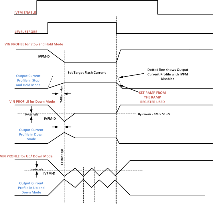 Figure 30. IVFM Modes
9.4.5 Fault/Protections
9.4.5.1 Fault Operation
If the LM3643 enters a fault condition, the device sets the appropriate flag in the Flags1 and Flags2 Registers (0x0A and 0x0B), and place the device into standby by clearing the Mode Bits ([1],[0]) in the Enable Register. The LM3643 remains in standby until an I2C read of the Flags1 and Flags2 Registers are completed. Upon clearing the flags/faults, the device can be restarted (Flash, Torch, IR, etc.). If the fault is still present, the LM3643 re-enters the fault state and enters standby again.
9.4.5.2 Flash Time-Out
The Flash Time-Out period sets the amount of time that the Flash Current is being sourced from the current sources (LED1/2). The LM3643 has 16 timeout levels ranging from 10 ms to 400 ms (see Timing Configuration Register (0x08) for more detail).
9.4.5.3 Overvoltage Protection (OVP)
The output voltage is limited to typically 5 V (see VOVP spec in the Electrical Characteristics). In situations such as an open LED, the LM3643 raises the output voltage in order to try and keep the LED current at its target value. When VOUT reaches 5 V (typ.) the overvoltage comparator trips and turns off the internal NFET. When VOUT falls below the “VOVP Off Threshold”, the LM3643 begins switching again. The mode bits are cleared, and the OVP flag is set, when an OVP condition is present for three rising OVP edges. This prevents momentary OVP events from forcing the device to shut down.
9.4.5.4 Current Limit
The LM3643 features two selectable inductor current limits that are programmable through the I2C-compatible interface. When the inductor current limit is reached, the LM3643 terminates the charging phase of the switching cycle. Switching resumes at the start of the next switching period. If the overcurrent condition persists, the device operates continuously in current limit.
Since the current limit is sensed in the NMOS switch, there is no mechanism to limit the current when the device operates in Pass Mode (current does not flow through the NMOS in pass mode). In Boost mode or Pass mode if VOUT falls below 2.3 V, the device stops switching, and the PFET operates as a current source limiting the current to 200 mA. This prevents damage to the LM3643 and excessive current draw from the battery during output short-circuit conditions. The mode bits are not cleared upon a Current Limit event, but a flag is set.
9.4.5.5 NTC Thermistor Input (Torch/Temp)
The TORCH/TEMP pin, when set to TEMP mode, serves as a threshold detector and bias source for negative temperature coefficient (NTC) thermistors. When the voltage at TEMP goes below the programmed threshold, the LM3643 is placed into standby mode. The NTC threshold voltage is adjustable from 200 mV to 900 mV in 100-mV steps. The NTC bias current is set to 50 µA. The NTC detection circuitry can be enabled or disabled via the Enable Register. If enabled, the NTC block turns on and off during the start and stop of a Flash/Torch event.
Additionally, the NTC input looks for an open NTC connection and a shorted NTC connection. If the NTC input falls below 100 mV, the NTC short flag is set, and the device is disabled. If the NTC input rises above 2.3 V, the NTC Open flag is set, and the device is disabled. These fault detections can be individually disabled/enabled via the NTC Open Fault Enable bit and the NTC Short Fault Enable bit.
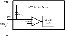 Figure 31. Temp Detection Diagram
9.4.5.6 Undervoltage Lockout (UVLO)
The LM3643 has an internal comparator that monitors the voltage at IN and forces the LM3643 into standby if the input voltage drops to 2.5 V. If the UVLO monitor threshold is tripped, the UVLO flag bit is set in the Flags1 Register (0x0A). If the input voltage rises above 2.5 V, the LM3643 is not available for operation until there is an I2C read of the Flags1 Register (0x0A). Upon a read, the Flags1 register is cleared, and normal operation can resume if the input voltage is greater than 2.5 V.
9.4.5.7 Thermal Shutdown (TSD)
When the LM3643 die temperature reaches 150°C, the thermal shutdown detection circuit trips, forcing the LM3643 into standby and writing a '1' to the corresponding bit of the Flags1 Register (0x0A) (Thermal Shutdown bit). The LM3643 is only allowed to restart after the Flags1 Register (0x0A) is read, clearing the fault flag. Upon restart, if the die temperature is still above 150°C, the LM3643 resets the Fault flag and re-enters standby.
9.4.5.8 LED and/or VOUT Short Fault
The LED Fault flags read back a '1' if the device is active in Flash or Torch mode and either active LED output experiences a short condition. The Output Short Fault flag reads back a '1' if the device is active in Flash or Torch mode and the boost output experiences a short condition. An LED short condition is determined if the voltage at LED1 or LED2 goes below 500 mV (typ.) while the device is in Torch or Flash mode. There is a deglitch time of 256 μs before the LED Short flag is valid and a deglitch time of 2.048 ms before the VOUT Short flag is valid. The LED Short Faults can be reset to '0' by removing power to the LM3643, setting HWEN to '0', setting the SW RESET bit to a '1', or by reading back the Flags1 Register (0x0A on LM3643). The mode bits are cleared upon an LED and/or VOUT short fault.
9.5 Programming
9.5.1 Control Truth Table
| MODE1 | MODE0 | STROBE EN | TORCH EN | STROBE PIN | TORCH PIN | ACTION |
|---|---|---|---|---|---|---|
| 0 | 0 | 0 | 0 | X | X | Standby |
| 0 | 0 | 0 | 1 | X | pos edge | Ext Torch |
| 0 | 0 | 1 | 0 | pos edge | X | Ext Flash |
| 0 | 0 | 1 | 1 | 0 | pos edge | Standalone Torch |
| 0 | 0 | 1 | 1 | pos edge | 0 | Standalone Flash |
| 0 | 0 | 1 | 1 | pos edge | pos edge | Standalone Flash |
| 1 | 0 | X | X | X | X | Int Torch |
| 1 | 1 | X | X | X | X | Int Flash |
| 0 | 1 | 0 | X | X | X | IRLED Standby |
| 0 | 1 | 1 | X | 0 | X | IRLED Standby |
| 0 | 1 | 1 | X | pos edge | X | IRLED enabled |
9.5.2 I2C-Compatible Interface
9.5.2.1 Data Validity
The data on SDA must be stable during the HIGH period of the clock signal (SCL). In other words, the state of the data line can only be changed when SCL is LOW.
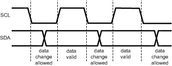 Figure 32. Data Validity Data
A pullup resistor between the controller's VIO line and SDA must be greater than [(VIO-VOL) / 3mA] to meet the VOL requirement on SDA. Using a larger pullup resistor results in lower switching current with slower edges, while using a smaller pullup results in higher switching currents with faster edges.
9.5.2.2 Start and Stop Conditions
START and STOP conditions classify the beginning and the end of the I2C session. A START condition is defined as the SDA signal transitioning from HIGH to LOW while SCL line is HIGH. A STOP condition is defined as the SDA transitioning from LOW to HIGH while SCL is HIGH. The I2C master always generates START and STOP conditions. The I2C bus is considered busy after a START condition and free after a STOP condition. During data transmission, the I2C master can generate repeated START conditions. First START and repeated START conditions are equivalent, function-wise.
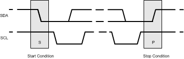 Figure 33. Start and Stop Conditions
9.5.2.3 Transferring Data
Every byte put on the SDA line must be eight bits long, with the most significant bit (MSB) transferred first. Each byte of data has to be followed by an acknowledge bit. The acknowledge related clock pulse is generated by the master. The master releases the SDA line (HIGH) during the acknowledge clock pulse. The LM3643 pulls down the SDA line during the 9th clock pulse, signifying an acknowledge. The LM3643 generates an acknowledge after each byte is received. There is no acknowledge created after data is read from the device.
After the START condition, the I2C master sends a chip address. This address is seven bits long followed by an eighth bit which is a data direction bit (R/W). The LM3643 7-bit address is 0x63. The device address for the LM3643A is 0x67. For the eighth bit, a '0' indicates a WRITE and a '1' indicates a READ. The second byte selects the register to which the data is written. The third byte contains data to write to the selected register.
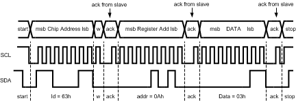 Figure 34. Write Cycle W = Write (SDA = "0") R = Read (SDA = "1") Ack = Acknowledge
 (SDA Pulled Down by Either Master or Slave) ID = Chip Address, 63h for LM3643
9.5.2.4 I2C-Compatible Chip Address
The device address for the LM3643 is 1100011 (0x63). The device address for the LM3643A is 1100111 (0x67).After the START condition, the I2C-compatible master sends the 7-bit address followed by an eighth read or write bit (R/W). R/W = 0 indicates a WRITE and R/W = 1 indicates a READ. The second byte following the device address selects the register address to which the data is written. The third byte contains the data for the selected register.
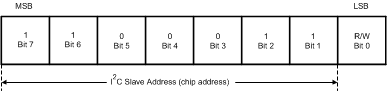 Figure 35. I2C-Compatible Chip Address
9.6 Register Descriptions
9.6.1 Enable Register (0x01)
| Bit 7 | Bit 6 | Bit 5 | Bit 4 | Bit 3 | Bit 2 | Bit 1 | Bit 0 |
|---|---|---|---|---|---|---|---|
| TX Pin Enable
0 = Disabled 1 = Enabled (Default ) |
Strobe Type
0 = Level Triggered (Default) 1 = Edge Triggered |
Strobe Enable
0 = Disabled (Default ) 1 = Enabled |
TORCH/TEMP Pin Enable
0 = Disabled (Default ) 1 = Enabled |
Mode Bits: M1, M0
'00' = Standby (Default) '01' = IR Drive '10' = Torch '11' = Flash |
LED2 Enable
0 = OFF (Default ) 1 = ON |
LED1 Enable
0 = OFF (Default) 1 = ON |
|
NOTE
Edge Strobe Mode is not valid in IR MODE. Switching between Level and Edge Strobe Types while the device is enabled is not recommended.
In Edge or Level Strobe Mode, it is recommended that the trigger pulse width be set greater than 1 ms to ensure proper turn-on of the device.
9.6.2 IVFM Register (0x02)
| Bit 7 | Bit 6 | Bit 5 | Bit 4 | Bit 3 | Bit 2 | Bit 1 | Bit 0 |
|---|---|---|---|---|---|---|---|
| RFU | UVLO Circuitry (Default)
0 = Disabled (Default) 1 = Enabled |
IVFM Levels
000 = 2.9 V (Default) 001 = 3 V 010 = 3.1 V 011 = 3.2 V 100 = 3.3 V 101 = 3.4 V 110 = 3.5 V 111 = 3.6 V |
IVFM Hysteresis
0 = 0 mV (Default) 1 = 50 mV |
IVFM Selection
00 = Disabled 01 = Stop and Hold Mode (Default) 10 = Down Mode 11 = Up and Down Mode |
|||
NOTE
IVFM Mode Bits are static once the LM3643 is enabled in Torch, Flash or IR modes. If the IVFM mode needs to be updated, disable the device and then change the mode bits to the desired state.
9.6.3 LED1 Flash Brightness Register (0x03)
| Bit 7 | Bit 6 | Bit 5 | Bit 4 | Bit 3 | Bit 2 | Bit 1 | Bit 0 |
|---|---|---|---|---|---|---|---|
| LED2 Flash Current Override
0 = LED2 Flash Current is not set to LED1 Flash Current 1 = LED2 Flash Current is set to LED1 Flash Current (Default) |
LED1 Flash Brightness Level
IFLASH1/2 (mA) ≈ (Brightness Code × 11.725 mA) + 10.9 mA 0000000 = 10.9 mA ....................... 0111111 = 729 mA (Default) ....................... 1111111 = 1.5 A |
||||||
9.6.4 LED2 Flash Brightness Register (0x04)
| Bit 7 | Bit 6 | Bit 5 | Bit 4 | Bit 3 | Bit 2 | Bit 1 | Bit 0 |
|---|---|---|---|---|---|---|---|
| RFU | LED2 Flash Brightness Levels
IFLASH1/2 (mA) ≈ (Brightness Code × 11.725 mA) + 10.9 mA 0000000 = 10.9 mA ....................... 0111111 = 729 mA (Default) ....................... 1111111 = 1.5 A |
||||||
9.6.5 LED1 Torch Brightness Register (0x05)
| Bit 7 | Bit 6 | Bit 5 | Bit 4 | Bit 3 | Bit 2 | Bit 1 | Bit 0 |
|---|---|---|---|---|---|---|---|
| LED2 Torch Current Override
0 = LED2 Torch Current is not set to LED1 Torch Current 1 = LED2 Torch Current is set to LED1 Torch Current (Default) |
LED1 Torch Brightness Levels
ITORCH1/2 (mA) ≈ (Brightness Code × 1.4 mA) + 0.977 mA 0000000 = 0.977 mA ....................... 0111111 = 89.3 mA (Default) ....................... 1111111 = 179 mA |
||||||
9.6.6 LED2 Torch Brightness Register (0x06)
| Bit 7 | Bit 6 | Bit 5 | Bit 4 | Bit 3 | Bit 2 | Bit 1 | Bit 0 |
|---|---|---|---|---|---|---|---|
| RFU | LED2 Torch Brightness Levels
ITORCH1/2 (mA) ≈ (Brightness Code × 1.4 mA) + 0.977 mA 0000000 = 0.977 mA ....................... 0111111 = 89.3 mA (Default) ....................... 1111111 = 179 mA |
||||||
9.6.7 Boost Configuration Register (0x07)
| Bit 7 | Bit 6 | Bit 5 | Bit 4 | Bit 3 | Bit 2 | Bit 1 | Bit 0 |
|---|---|---|---|---|---|---|---|
| Software Reset Bit
0 = Not Reset (Default) 1 = Reset |
RFU | RFU | RFU | LED Pin Short Fault Detect
0 = Disabled 1 = Enabled (Default) |
Boost Mode
0 = Normal (Default) 1 = Pass Mode Only |
Boost Frequency Select
0 = 2 MHz (Default) 1 = 4 MHz |
Boost Current Limit Setting
0 = 1.9 A 1 = 2.8 A (Default) |
9.6.8 Timing Configuration Register (0x08)
| Bit 7 | Bit 6 | Bit 5 | Bit 4 | Bit 3 | Bit 2 | Bit 1 | Bit 0 |
|---|---|---|---|---|---|---|---|
| RFU | Torch Current Ramp Time
000 = No Ramp 001 = 1 ms (Default) 010 = 32 ms 011 = 64 ms 100 = 128 ms 101 = 256 ms 110 = 512 ms 111 = 1024 ms |
Flash Time-Out Duration
0000 = 10 ms 0001 = 20 ms 0010 = 30 ms 0011 = 40 ms 0100 = 50 ms 0101 = 60 ms 0110 = 70 ms 0111 = 80 ms 1000 = 90 ms 1001 = 100 ms 1010 = 150 ms (Default) 1011 = 200 ms 1100 = 250 ms 1101 = 300 ms 1110 = 350 ms 1111 = 400 ms |
|||||
9.6.9 TEMP Register (0x09)
| Bit 7 | Bit 6 | Bit 5 | Bit 4 | Bit 3 | Bit 2 | Bit 1 | Bit 0 |
|---|---|---|---|---|---|---|---|
| RFU | TORCH Polarity
0 = Active High (Default) (Pulldown Resistor Enabled) 1 = Active Low (Pulldown Resistor Disabled) |
NTC Open Fault Enable
0 = Disabled (Default) 1 =Enable |
NTC Short Fault Enable
0 = Disabled (Default) 1 =Enable |
TEMP Detect Voltage Threshold
000 = 0.2 V 001 = 0.3 V 010 = 0.4 V 011 = 0.5 V 100 = 0.6 V (Default) 101 = 0.7 V 110 = 0.8 V 111 = 0.9 V |
TORCH/TEMP
Function Select 0 = TORCH (Default) 1 = TEMP |
||
NOTE
The Torch Polarity bit is static once the LM3643 is enabled in Torch, Flash or IR modes. If the Torch Polarity bit needs to be updated, disable the device and then change the Torch Polarity bit to the desired state.
9.6.10 Flags1 Register (0x0A)
| Bit 7 | Bit 6 | Bit 5 | Bit 4 | Bit 3 | Bit 2 | Bit 1 | Bit 0 |
|---|---|---|---|---|---|---|---|
| TX Flag | VOUT Short Fault | VLED1 Short Fault | VLED2 Short Fault | Current Limit Flag | Thermal Shutdown (TSD) Fault | UVLO Fault | Flash Time-Out Flag |
9.6.11 Flags2 Register (0x0B)
| Bit 7 | Bit 6 | Bit 5 | Bit 4 | Bit 3 | Bit 2 | Bit 1 | Bit 0 |
|---|---|---|---|---|---|---|---|
| RFU | RFU | RFU | NTC Short Fault | NTC Open Fault | IVFM Trip Flag | OVP Fault | TEMP Trip Fault |
9.6.12 Device ID Register (0x0C)
9.6.13 Last Flash Register (0x0D)
| Bit 7 | Bit 6 | Bit 5 | Bit 4 | Bit 3 | Bit 2 | Bit 1 | Bit 0 |
|---|---|---|---|---|---|---|---|
| RFU | The value stored is always the last current value the IVFM detection block set. ILED = IFLASH-TARGET × ((Code + 1) / 128) | ||||||