SNVS967A August 2014 – November 2014 LM3643
PRODUCTION DATA.
- 1 Features
- 2 Applications
- 3 Description
- 4 Simplified Schematic
- 5 Revision History
- 6 Device Comparison Table
- 7 Pin Configuration and Functions
- 8 Specifications
-
9 Detailed Description
- 9.1 Overview
- 9.2 Functional Block Diagram
- 9.3 Feature Description
- 9.4 Device Functioning Modes
- 9.5 Programming
- 9.6
Register Descriptions
- 9.6.1 Enable Register (0x01)
- 9.6.2 IVFM Register (0x02)
- 9.6.3 LED1 Flash Brightness Register (0x03)
- 9.6.4 LED2 Flash Brightness Register (0x04)
- 9.6.5 LED1 Torch Brightness Register (0x05)
- 9.6.6 LED2 Torch Brightness Register (0x06)
- 9.6.7 Boost Configuration Register (0x07)
- 9.6.8 Timing Configuration Register (0x08)
- 9.6.9 TEMP Register (0x09)
- 9.6.10 Flags1 Register (0x0A)
- 9.6.11 Flags2 Register (0x0B)
- 9.6.12 Device ID Register (0x0C)
- 9.6.13 Last Flash Register (0x0D)
- 10Applications and Implementation
- 11Power Supply Recommendations
- 12Layout
- 13Device and Documentation Support
- 14Mechanical, Packaging, and Orderable Information
Package Options
Mechanical Data (Package|Pins)
- YFF|12
Thermal pad, mechanical data (Package|Pins)
Orderable Information
7 Pin Configuration and Functions
DSBGA
12 Pins
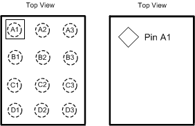
Pin Functions
| PIN | DESCRIPTION | |
|---|---|---|
| NUMBER | NAME | |
| A1 | GND | Ground |
| A2 | IN | Input voltage connection. Connect IN to the input supply and bypass to GND with a 10-µF or larger ceramic capacitor. |
| A3 | SDA | Serial data input/output in the I2C Mode on LM3643. |
| B1 | SW | Drain Connection for Internal NMOS and Synchronous PMOS Switches. |
| B2 | STROBE | Active high hardware flash enable. Drive STROBE high to turn on Flash pulse. Internal pulldown resistor of 300 kΩ between STROBE and GND. |
| B3 | SCL | Serial clock input for LM3643. |
| C1 | OUT | Step-up DC/DC Converter Output. Connect a 10-µF ceramic capacitor between this terminal and GND. |
| C2 | HWEN | Active high enable pin. High = Standby, Low = Shutdown/Reset. Internal pulldown resistor of 300 kΩ between HWEN and GND. |
| C3 | TORCH/TEMP | Torch terminal input or threshold detector for NTC temperature sensing and current scale back. |
| D1 | LED2 | High-side current source output for flash LED. |
| D2 | TX | Configurable dual polarity power amplifier synchronization input. Internal pulldown resistor of 300 kΩ between TX and GND. |
| D3 | LED1 | High-side current source output for flash LED. |