SNVS449O June 2007 – April 2015 LM3668
PRODUCTION DATA.
- 1 Features
- 2 Applications
- 3 Description
- 4 Revision History
- 5 Device Comparison Table
- 6 Pin Configuration and Functions
- 7 Specifications
- 8 Detailed Description
- 9 Application and Implementation
- 10Power Supply Recommendations
- 11Layout
- 12Device and Documentation Support
- 13Mechanical, Packaging, and Orderable Information
Package Options
Mechanical Data (Package|Pins)
- DQB|12
Thermal pad, mechanical data (Package|Pins)
Orderable Information
1 Features
- 45-µA Typical Quiescent Current
- For 2.8-V-3.3-V and 3-V-3.4-V Versions:
- 1-A Maximum Load Current for
VIN = 2.8 V to 5.5 V - 800-mA Maximum Load Current for
VIN = 2.7 V - 600-mA Maximum Load Current for
VIN = 2.5 V
- 1-A Maximum Load Current for
- For 4.5 V-5 V
- 1-A Maximum Load Current for
VIN = 3.9 V to 5.5 V - 800-mA Maximum Load Current for
VIN = 3.4 V to 3.8 V - 700-mA Maximum Load Current for
VIN = 3 V to 3.3 V - 600-mA Maximum Load Current for
VIN = 2.7 V to 2.9 V
- 1-A Maximum Load Current for
- 2.2-MHz PWM Fixed Switching Frequency (Typical)
- Automatic PFM-PWM Mode or Forced PWM Mode
- Wide Input Voltage Range: 2.5 V to 5.5 V
- Internal Synchronous Rectification for High Efficiency
- Internal Soft Start: 600-µs Maximum Start-Up Time After VIN Settled
- 0.01-µA Typical Shutdown Current
- Current Overload and Thermal Shutdown Protection
- Frequency Sync Pin: 1.6 MHz to 2.7 MHz
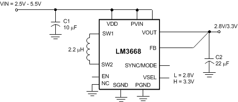
Typical Application Circuit

2 Applications
- Handset Peripherals
- MP3 Players
- Pre-Regulation for Linear Regulators
- PDAs
- Portable Hard Disk Drives
- WiMax Modems
3 Description
The LM3668 is a synchronous buck-boost DC-DC converter optimized for powering low voltage circuits from a Li-Ion battery and input voltage rails between 2.5 V and 5.5 V. It has the capability to support up to 1-A output current over the output voltage range. The LM3668 regulates the output voltage over the complete input voltage range by automatically switching between buck or boost modes depending on the input voltage.
The LM3668 has 2 N-channel MOSFETS and 2 P-channel MOSFETS arranged in a topology that provides continuous operation through the buck and boost operating modes. There is a MODE pin that allows the user to choose between an intelligent automatic PFM-PWM mode operation and forced PWM operation. During PWM mode, a fixed-frequency 2.2 MHz (typical) is used. PWM mode drives load up to 1 A. Hysteretic PFM mode extends the battery life through reduction of the quiescent current to 45 µA (typical) at light loads during system standby. Internal synchronous rectification provides high efficiency. In shutdown mode (EN pin pulled low), the device turns off and reduces battery consumption to 0.01 µA (typical).
A high switching frequency of 2.2 MHz (typical) allows the use of tiny surface-mount components including a 2.2-µH inductor, a 10-µF input capacitor, and a 22-µF output capacitor.
Device Information(1)
| PART NUMBER | PACKAGE | BODY SIZE (NOM) |
|---|---|---|
| LM3668 | WSON (12) | 3.00 mm x 3.00 mm |
- For all available packages, see the orderable addendum at the end of the datasheet.
4 Revision History
Changes from N Revision (August 2014) to O Revision
- Changed RθJA value from 34 to 47.3; change 20 PINS to 12 PINS in header; add additional thermal informationGo
Changes from M Revision (May 2013) to N Revision
- Added Pin Configuration and Functions section, Handling Rating table, Feature Description section, Device Functional Modes, Application and Implementation section, Power Supply Recommendations section, Layout section, Device and Documentation Support section, and Mechanical, Packaging, and Orderable Information section Go
Changes from L Revision (April 2013) to M Revision
- Changed layout of National Data Sheet to TI formatGo