SNVS449O June 2007 – April 2015 LM3668
PRODUCTION DATA.
- 1 Features
- 2 Applications
- 3 Description
- 4 Revision History
- 5 Device Comparison Table
- 6 Pin Configuration and Functions
- 7 Specifications
- 8 Detailed Description
- 9 Application and Implementation
- 10Power Supply Recommendations
- 11Layout
- 12Device and Documentation Support
- 13Mechanical, Packaging, and Orderable Information
Package Options
Mechanical Data (Package|Pins)
- DQB|12
Thermal pad, mechanical data (Package|Pins)
Orderable Information
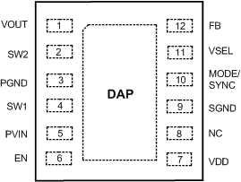
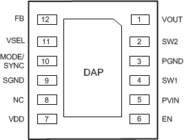
6 Pin Configuration and Functions
DQB Package
12-Pin WSON
Top View

DQB Package
12-Pin WSON
Bottom View

Pin Functions(1)
| PIN | TYPE | DESCRIPTION | |
|---|---|---|---|
| NO. | NAME | ||
| 1 | VOUT | A | Connect to output capacitor. |
| 2 | SW2 | A | Switching node connection to the internal PFET switch (P2) and NFET synchronous rectifier (N2). |
| 3 | PGND | G | Power ground. |
| 4 | SW1 | A | Switching node connection to the internal PFET switch (P1) and NFET synchronous rectifier (N1). |
| 5 | PVIN | P | Supply to the power switch, connect to the input capacitor. |
| 6 | EN | I | Enable input. Set this digital input high for normal operation. For shutdown, set low. |
| 7 | VDD | P | Signal supply input. If board layout is not optimum an optional 1-µF ceramic capacitor is suggested as close to this pin as possible. |
| 8 | NC | - | No connect. Connect this pin to SGND on PCB layout. |
| 9 | SGND | G | Analog and Control Ground. |
| 10 | MODE/SYNC | I | Mode = LOW, Automatic Mode. Mode= HI, forced PWM Mode. SYNC = external clock synchronization from 1.6 MHz to 2.7 MHz.(When SYNC function is used, device is forced in PWM mode). |
| 11 | VSEL | I | Voltage selection pin; (for example, 2.8-V-3.3-V option) logic input low (or GND) = 2.8 V and logic high = 3.3 V (or VIN) to set output voltage. |
| 12 | FB | A | Feedback analog input. Connect to the output at the output filter. |
| DAP | DAP | - | Die Attach Pad, connect the DAP to SGND on PCB layout to enhance thermal performance. It should not be used as a primary ground connection. |
(1) A: Analog Pin, G: Ground Pin, P: Power Pin, I: Digital Input Pin