SNVS449O June 2007 – April 2015 LM3668
PRODUCTION DATA.
- 1 Features
- 2 Applications
- 3 Description
- 4 Revision History
- 5 Device Comparison Table
- 6 Pin Configuration and Functions
- 7 Specifications
- 8 Detailed Description
- 9 Application and Implementation
- 10Power Supply Recommendations
- 11Layout
- 12Device and Documentation Support
- 13Mechanical, Packaging, and Orderable Information
Package Options
Mechanical Data (Package|Pins)
- DQB|12
Thermal pad, mechanical data (Package|Pins)
Orderable Information
9 Application and Implementation
NOTE
Information in the following applications sections is not part of the TI component specification, and TI does not warrant its accuracy or completeness. TI’s customers are responsible for determining suitability of components for their purposes. Customers should validate and test their design implementation to confirm system functionality.
9.1 Application Information
9.1.1 MODE/SYNC Pin
If the MODE/SYNC pin is set high, the device is set to operate at PWM mode only. If MODE/SYNC pin is set low, the device is set to automatically transition from PFM to PWM or PWM to PFM depending on the load current. Do not leave this pin floating. The MODE/SYNC pin can also be driven by an external clock to set the desired switching frequency between 1.6 MHz to 2.7 MHz.
9.1.2 VSEL Pin
The LM3668 has built in logic for conveniently setting the output voltage, for example if VVSEL high, the output is set to 3.3 V; with VVSEL low the output is set to 2.8 V. It is not recommended to use this function for dynamically switching between 2.8 V and 3.3 V or switching at maximum load.
9.2 Typical Application
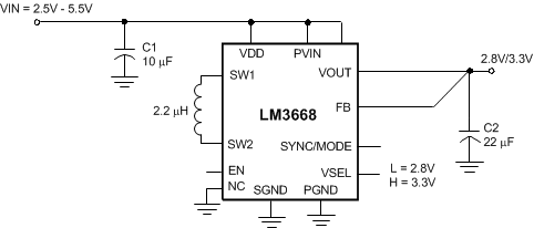 Figure 46. LM3668 Typical Application Circuit
9.2.1 Design Requirements
9.2.1.1 Maximum Current
The LM3668 is designed to operate up to 1 A. For input voltages at 2.5 V, the maximum operating current is 600 mA and 800 mA for 2.7 V input voltage. In any mode it is recommended to avoid starting up the device at minimum input voltage and maximum load. Special attention must be taken to avoid operating near thermal shutdown when operating in boost mode at maximum load (1 A). A simple calculation can be used to determine the power dissipation at the operating condition; PD-MAX = (TJ-MAX-OP – TA-MAX)/RθJA. The LM3668 has thermal resistance RθJA = 47.3°C/W (see Thermal Information and maximum operating ambient of 85°C. As a result, the maximum power dissipation using the above formula is around 845 mW.
9.2.2 Detailed Design Procedure
9.2.2.1 Inductor Selection
There are two main considerations when choosing an inductor: the inductor should not saturate, and the inductor current ripple should be small enough to achieve the desired output voltage ripple. Different saturation current rating specifications are followed by different manufacturers so attention must be given to details. Saturation current ratings are typically specified at 25°C. However, ratings at the maximum ambient temperature of application should be requested from the manufacturer. Shielded inductors radiate less noise and should be preferred.
In the case of the LM3668, there are two modes (Buck & Boost) of operation that must be consider when selecting an inductor with appropriate saturation current. The saturation current should be greater than the sum of the maximum load current and the worst case average to peak inductor current. Equation 1 shows the buck mode operation for worst case conditions and the second equation for boost condition.
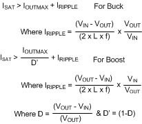
where
- IRIPPLE: Peak inductor current
- IOUTMAX: Maximum load current
- VIN: Maximum input voltage in application
- L : Min inductor value including worst case tolerances (30% drop can be considered)
- f : Minimum switching frequency
- VOUT: Output voltage
- D: Duty Cycle for CCM Operation
- VOUT : Output voltage
- VIN: Input voltage
- VIN = 2.8 V to 4 V
- VOUT = 3.3 V
- IOUT = 500 mA
- L = 2.2 µH
- F = 2 MHz
- Buck: ISAT = 567 mA
- Boost: ISAT = 638 mA
As a result, the inductor should be selected according to the highest of the two ISAT values.
A more conservative and recommended approach is to choose an inductor that has a saturation current rating greater than the maximum current limit of 2.05 A.
A 2.2-µH inductor with a saturation current rating of at least 2.05 A is recommended for most applications. The inductor’s resistance should be less than 100 mΩ for good efficiency. For low-cost applications, an unshielded bobbin inductor could be considered. For noise critical applications, a toroidal or shielded-bobbin inductor should be used. A good practice is to lay out the board with overlapping footprints of both types for design flexibility. This allows substitution of a low-noise shielded inductor, in the event that noise from low-cost bobbin model is unacceptable.
Table 2. Suggest Inductors and Suppliers
| MODEL | VENDOR | DIMENSIONS
LxWxH (mm) |
D.C.R (mΩ)(MAX) | ISAT (A) |
|---|---|---|---|---|
| LPS4012-222L | Coilcraft | 4 x 4 x 1.2 | 100 | 2.1 |
| LPS4018-222L | Coilcraft | 4 x 4 x 1.8 | 70 | 2.5 |
| 1098AS-2R0M (2 µH) | TOKO | 3 x 2.8 x 1.2 | 67 | 1.8 (lower current applications) |
9.2.2.2 Input Capacitor Selection
A ceramic input capacitor of at least 10 µF, 6.3 V is sufficient for most applications. Place the input capacitor as close as possible to the PVIN pin of the device. A larger value may be used for improved input voltage filtering. Use X7R or X5R types; do not use Y5V . DC bias characteristics of ceramic capacitors must be considered when selecting case sizes like 0805 or 0603. The input filter capacitor supplies current to the PFET switch of the LM3668 in the first half of each cycle and reduces voltage ripple imposed on the input power source. A ceramic capacitor’s low ESR provides the best noise filtering of the input voltage spikes due to this rapidly changing current. For applications where input voltage is 4 V or higher, it is best to use a higher voltage rating capacitor to eliminate the DC bias affect over capacitance.
9.2.2.3 Output Capacitor Selection
A ceramic output capacitor of 22 µF, 6.3 V (use 10 V or higher rating for 4.5 V-5 V output option) is sufficient for most applications. Multilayer ceramic capacitors such as X7R or X5R with low ESR is a good choice for this as well. These capacitors provide an ideal balance between small size, cost, reliability and performance. Do not use Y5V ceramic capacitors as they have temperature limitation and poor dielectric performance over temperature and poor voltage characteristic for a given value. In other words, ensure the minimum COUT value does not exceed −40% of the above-suggested value over the entire range of operating temperature and bias conditions.
Extra attention is required if a smaller case size capacitor is used in the application. Smaller case size capacitors typically have less capacitance for a given bias voltage as compared to a larger case size capacitor with the same bias voltage. Please contact the capacitor manufacturer for detailed information regarding capacitance verses case size. Table 3 lists several capacitor suppliers.
The output filter capacitor smooths out current flow from the inductor to the load, helps maintain a steady output voltage during transient load changes and reduces output voltage ripple. These capacitors must be selected with sufficient capacitance and sufficiently low ESR to perform these functions.
Note that the output voltage ripple is dependent on the inductor current ripple and the equivalent series resistance of the output capacitor (RESR).
The RESR is frequency dependent (as well as temperature dependent); make sure the value used for calculations is at the switching frequency of the part.
Table 3. Suggested Capacitors and Suppliers
| MODEL | TYPE | VENDOR | VOLTAGE RATING (V) | CASE SIZE INCH (mm) |
|---|---|---|---|---|
| 10 µF FOR CIN (FOR 4.5/5 V OPTION, USE 10 V OR HIGHER RATING CAPACITOR) | ||||
| GRM21BR60J106K | Ceramic, X5R | Murata | 6.3 | 0805 (2012) |
| JMK212BJ106K | Ceramic, X5R | Taiyo-Yuden | 6.3 | 0805 (2012) |
| C2012X5R0J106K | Ceramic, X5R | TDK | 6.3 | 0805 (2012) |
| LMK212 BJ106MG (±20%) | Ceramic, X5R | Taiyon-Yuden | 10 | 0806(2012) |
| LMK212 BJ106KG (±10%) | Ceramic, X5R | Taiyon-Yuden | 10 | 0805(2012) |
| 22 µF FOR COUT (FOR 4.5/5 V OPTION, USE 10 V OR HIGHER RATING CAPACITOR) | ||||
| JMK212BJ226MG | Ceramic, X5R | Taiyo-Yuden | 6.3 | 0805 (2012) |
| LMK212BJ226MG | Ceramic, X5R | Taiyo-Yuden | 10 | 0805 (2012) |
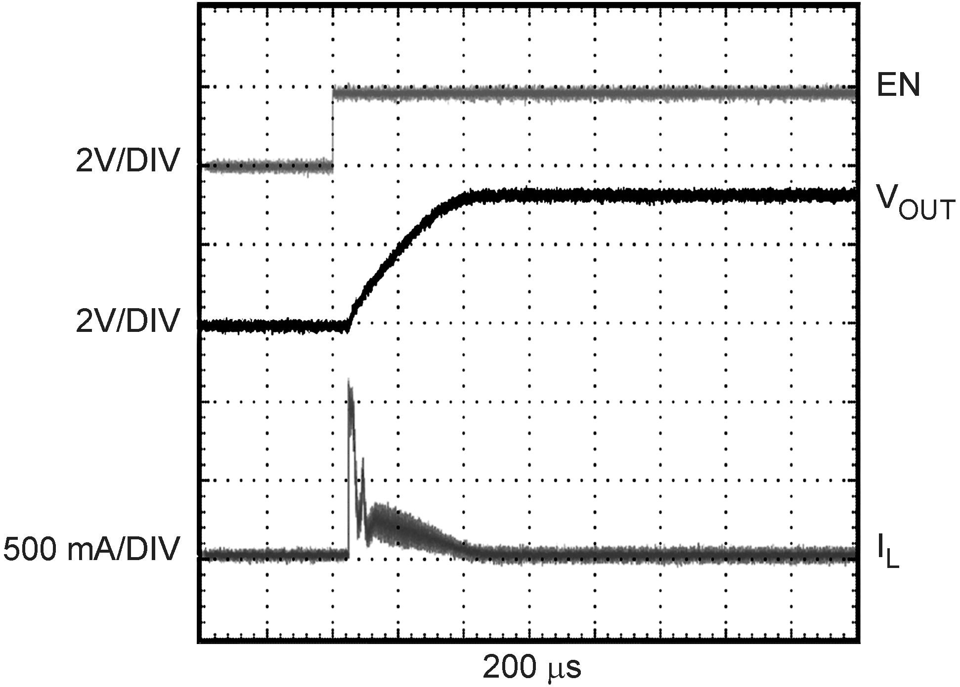
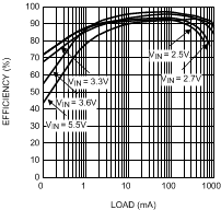
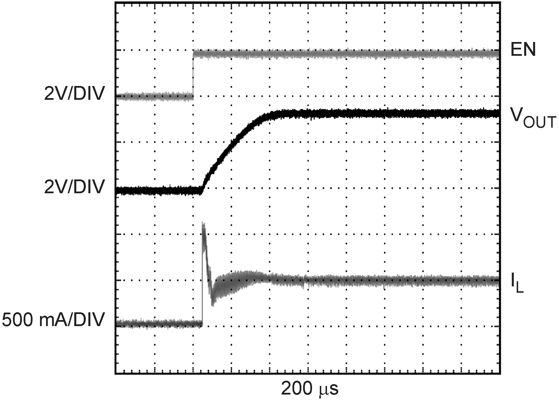
9.2.3 Application Curves
