SNVS114G May 1999 – February 2015 LM3940
PRODUCTION DATA.
- 1 Features
- 2 Applications
- 3 Description
- 4 Revision History
- 5 Pin Configuration and Functions
- 6 Specifications
- 7 Detailed Description
- 8 Application and Implementation
- 9 Power Supply Recommendations
- 10Layout
- 11Device and Documentation Support
- 12Mechanical, Packaging, and Orderable Information
Package Options
Mechanical Data (Package|Pins)
Thermal pad, mechanical data (Package|Pins)
Orderable Information
6 Specifications
6.1 Absolute Maximum Ratings
over operating free-air temperature range (unless otherwise noted)(1)| MIN | MAX | UNIT | |
|---|---|---|---|
| Power dissipation(2) | Internally Limited | ||
| Input supply voltage | –0.3 | 7.5 | V |
| Storage temperature, Tstg | −65 | 150 | °C |
(1) Stresses beyond those listed under Absolute Maximum Ratings may cause permanent damage to the device. These are stress ratings only, which do not imply functional operation of the device at these or any other conditions beyond those indicated under Recommended Operating Conditions. Exposure to absolute-maximum-rated conditions for extended periods may affect device reliability.
(2) The maximum allowable power dissipation is a function of the maximum junction temperature, TJ, the junction-to-ambient thermal resistance, RθJA, and the ambient temperature, TA. Exceeding the maximum allowable power dissipation will cause excessive die temperature, and the regulator will go into thermal shutdown. The value of RθJA (for devices in still air with no heatsink) is 23.3°C/W for the TO-220 package, 40.9°C/W for the DDPAK/TO-263 package, and 59.3°C/W for the SOT-223 package. The effective value of RθJA can be reduced by using a heatsink (see Heatsinking for specific information on heatsinking).
6.2 ESD Ratings
| VALUE | UNIT | |||
|---|---|---|---|---|
| V(ESD) | Electrostatic discharge | Human-body model (HBM), per ANSI/ESDA/JEDEC JS-001(1) | ±2000 | V |
| Charged-device model (CDM), per JEDEC specification JESD22-C101(2) | ±500 | |||
(1) JEDEC document JEP155 states that 500-V HBM allows safe manufacturing with a standard ESD control process.
(2) JEDEC document JEP157 states that 250-V CDM allows safe manufacturing with a standard ESD control process.
6.3 Recommended Operating Conditions
over operating free-air temperature range (unless otherwise noted)| MIN | MAX | UNIT | |
|---|---|---|---|
| Junction temperature, TJ | –40 | 125 | °C |
| Input supply voltage, VIN | 4.5 | 5.5 | V |
6.4 Thermal Information
| THERMAL METRIC(1) | LM3940 | UNIT | |||
|---|---|---|---|---|---|
| SOT-223 (DCY) | TO-263 (KTT) | TO-220 (NDE) | |||
| 4 PINS | 3 PINS | 3 PINS | |||
| RθJA | Junction-to-ambient thermal resistance, High-K | 59.3 | 40.9 | 23.3 | °C/W |
| RθJC(top) | Junction-to-case (top) thermal resistance | 38.9 | 43.5 | 16.1 | °C/W |
| RθJB | Junction-to-board thermal resistance | 8.1 | 23.5 | 4.8 | °C/W |
| ψJT | Junction-to-top characterization parameter | 1.7 | 10.3 | 2.7 | °C/W |
| ψJB | Junction-to-board characterization parameter | 8.0 | 22.5 | 4.8 | °C/W |
| RθJC(bot) | Junction-to-case (bottom) thermal resistance | n/a | 0.8 | 1.1 | °C/W |
(1) For more information about traditional and new thermal metrics, see the IC Package Thermal Metrics application report, SPRA953.
6.5 Electrical Characteristics
Over operating free-air temperature range, VIN = 5 V, IOUT = 1 A, COUT = 33 μF (unless otherwise noted). Limits apply for TJ = 25°C, unless otherwise specified in the Test Conditions column.(1)| PARAMETER | TEST CONDITIONS | MIN | TYP | MAX | UNIT | |
|---|---|---|---|---|---|---|
| VOUT | Output voltage | 5 mA ≤ IOUT ≤ 1 A, TJ = 25°C | 3.20 | 3.3 | 3.40 | V |
| 5 mA ≤ IOUT ≤ 1 A, –40°C ≤ TJ ≤ 125°C |
3.13 | 3.47 | ||||
 |
Line regulation | IOUT = 5 mA 4.5 V ≤ VIN ≤ 5.5 V |
20 | 40 | mV | |
 |
Load regulation | 50 mA ≤ IOUT ≤ 1 A, TJ = 25°C | 35 | 50 | ||
| 50 mA ≤ IOUT ≤ 1 A –40°C ≤ TJ ≤ 125°C |
35 | 80 | ||||
| ZOUT | Output impedance | IOUT (DC) = 100 mA IOUT (AC) = 20 mA (rms) ƒ = 120 Hz |
35 | mΩ | ||
| IQ | Quiescent current | 4.5 V ≤ VIN ≤ 5.5 V, IOUT = 5 mA, TJ = 25°C | 10 | 15 | mA | |
| 4.5 V ≤ VIN ≤ 5.5 V, IOUT = 5 mA –40°C ≤ TJ ≤ 125°C |
10 | 20 | ||||
| VIN = 5 V, IOUT = 1 A, TJ = 25°C | 110 | 200 | ||||
| VIN = 5 V, IOUT = 1 A –40°C ≤ TJ ≤ 125°C |
110 | 250 | ||||
| en | Output noise voltage | ƒBW = 10 Hz – 100 kHz IOUT = 5 mA |
150 | μV(rms) | ||
| VDO | Dropout voltage(2) | IOUT = 1 A, TJ = 25°C | 0.5 | 0.8 | V | |
| IOUT = 1 A –40°C ≤ TJ ≤ 125°C |
0.5 | 1 | ||||
| IOUT = 100 mA, TJ = 25°C | 110 | 150 | mV | |||
| IOUT = 100 mA –40°C ≤ TJ ≤ 125°C |
110 | 200 | ||||
| IOUT(SC) | Short-circuit current | RL = 0 | 1.2 | 1.7 | A | |
(1) All limits specified for TJ = 25°C are 100% tested and are used to calculate Outgoing Quality Levels. All limits at temperature extremes are verified via correlation using standard Statistical Quality Control (SQC) methods.
(2) Dropout voltage is defined as the input-output differential voltage where the regulator output drops to a value that is 100 mV below the value that is measured at VIN = 5 V.
6.6 Typical Characteristics
At TJ=25°C, unless otherwise noted.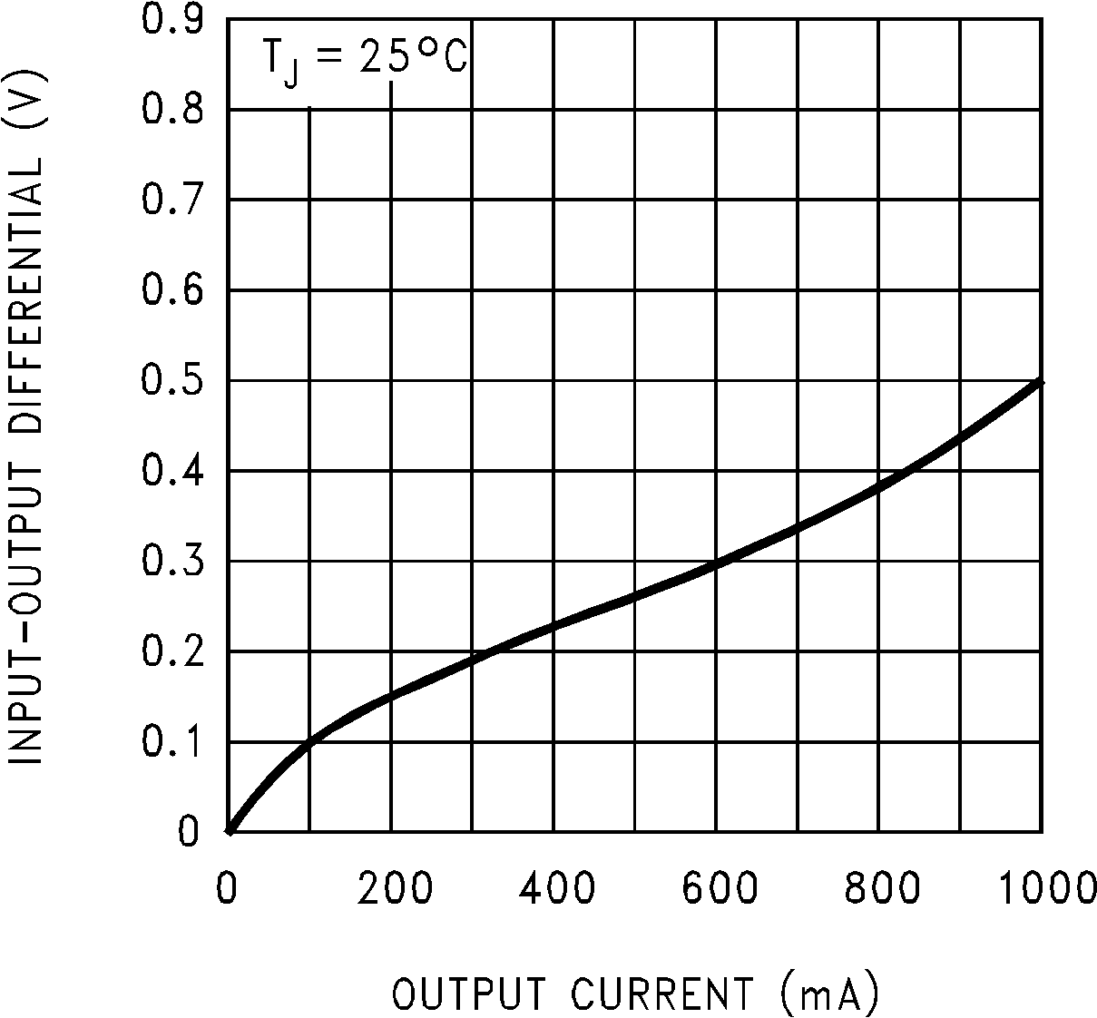 Figure 1. Dropout Voltage
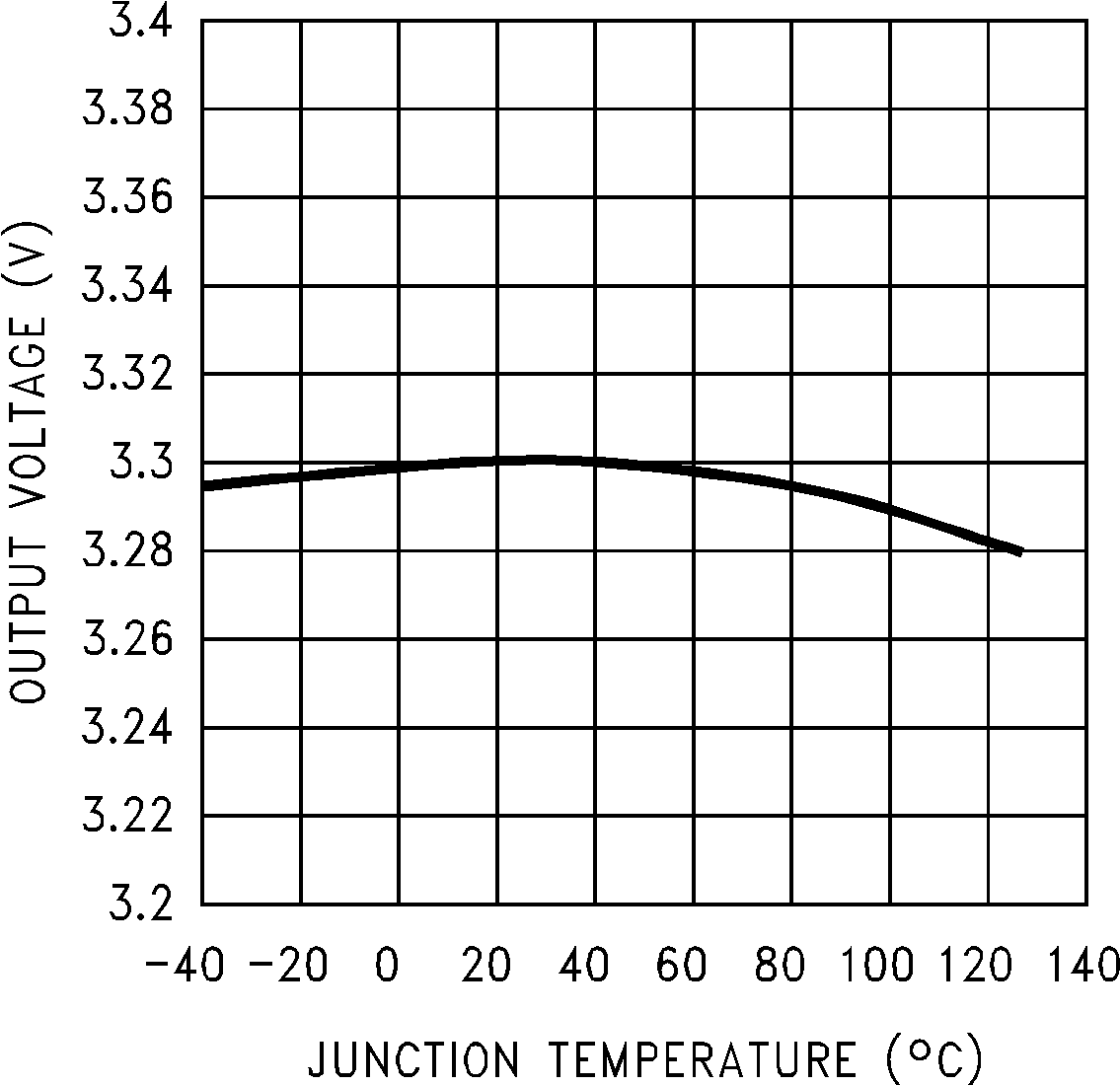 Figure 3. Output Voltage vs. Temperature
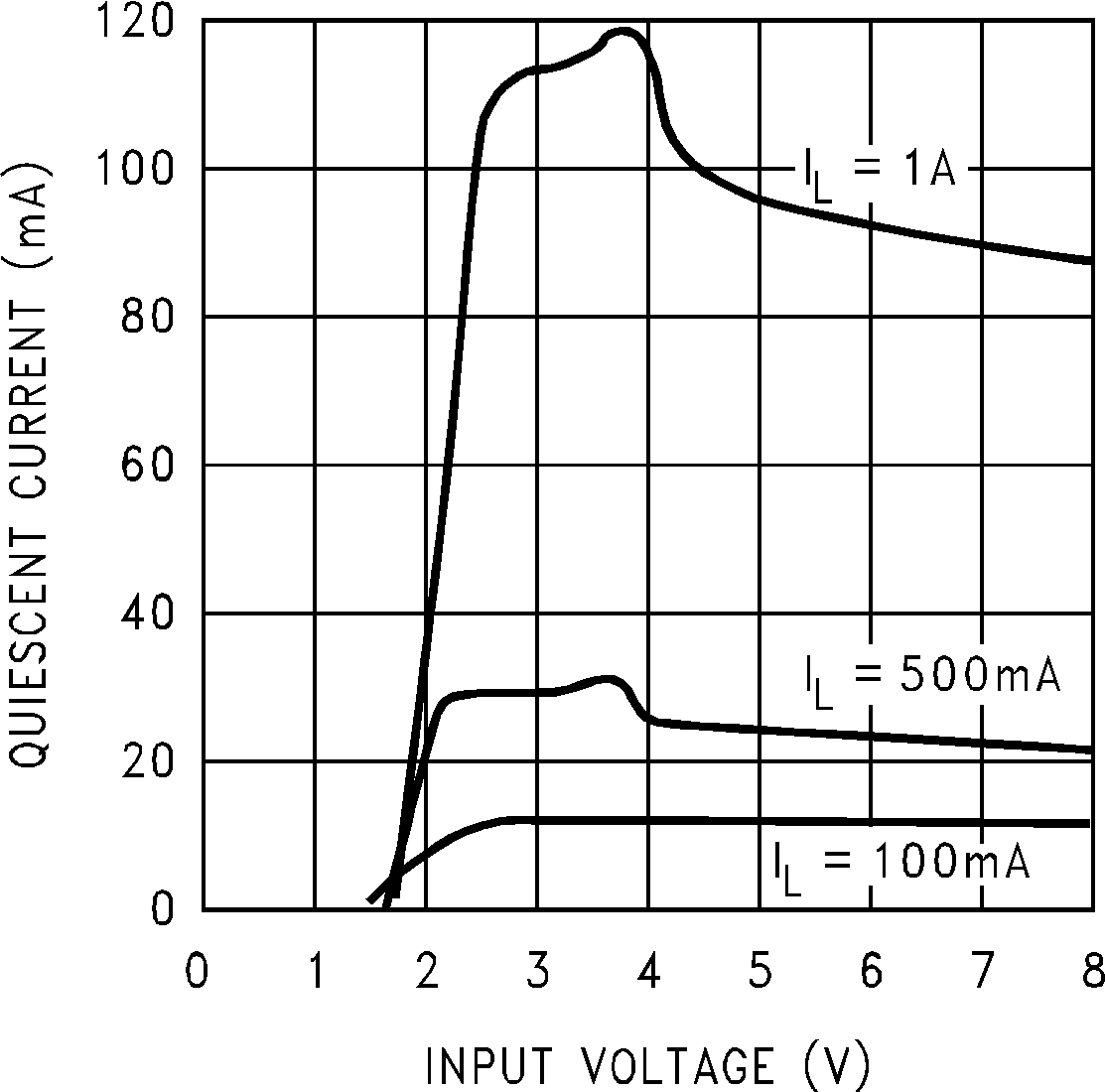 Figure 5. Quiescent Current vs. VIN
 Figure 7. Ripple Rejection
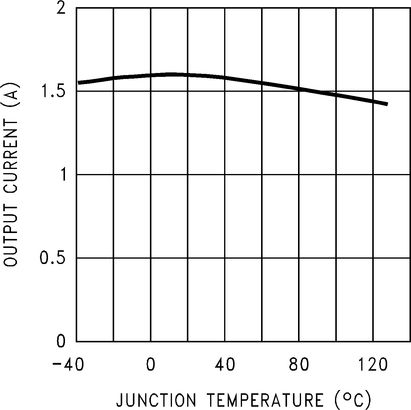 Figure 9. Peak Output Current
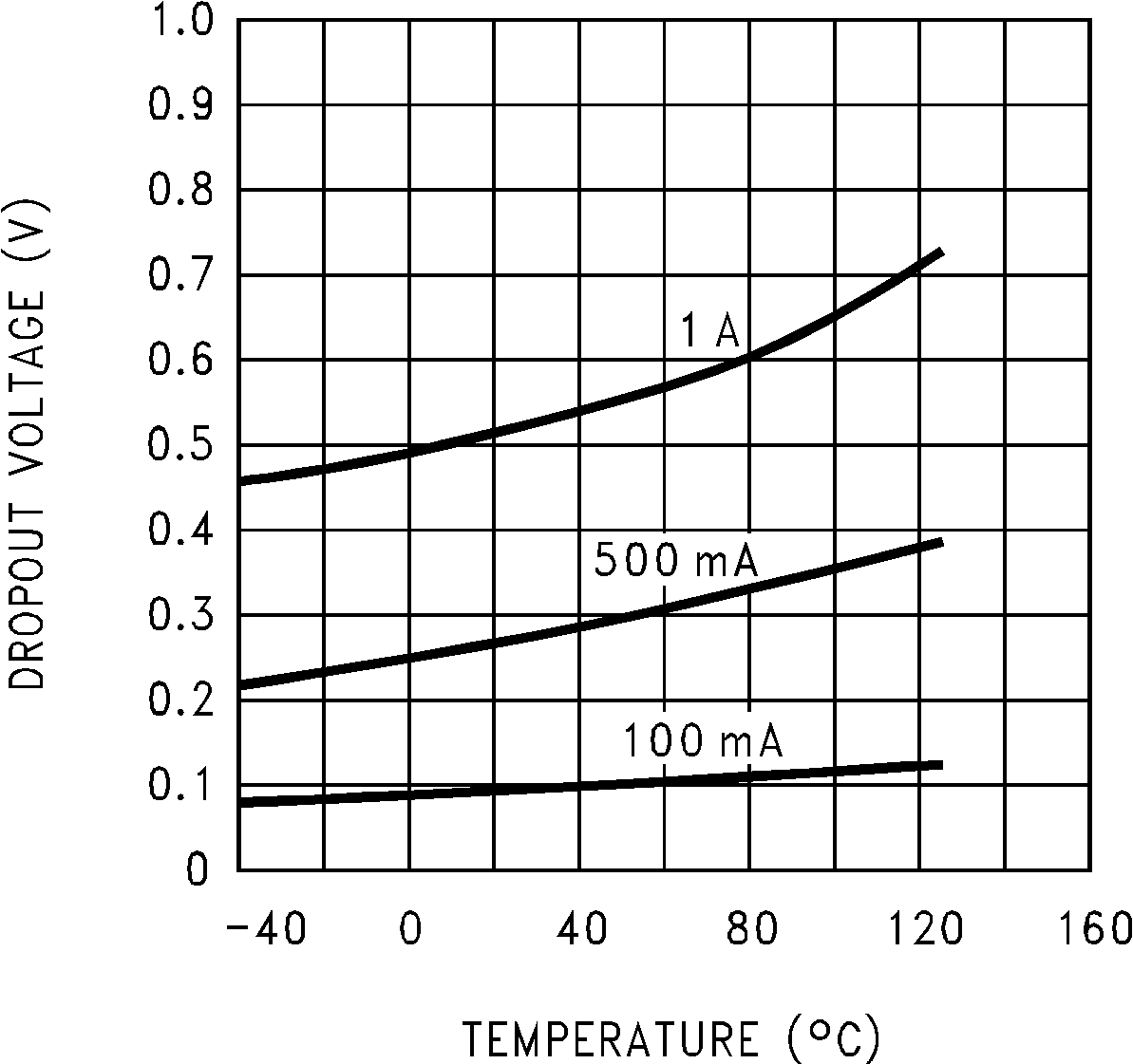 Figure 2. Dropout Voltage vs. Temperature
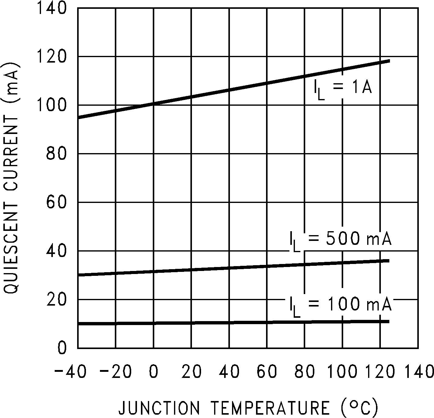 Figure 4. Quiescent Current vs. Temperature
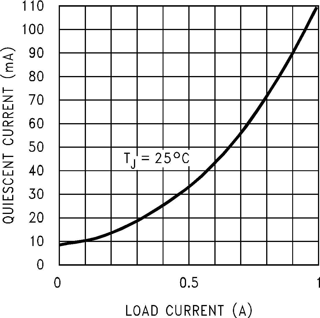 Figure 6. Quiescent Current vs. Load
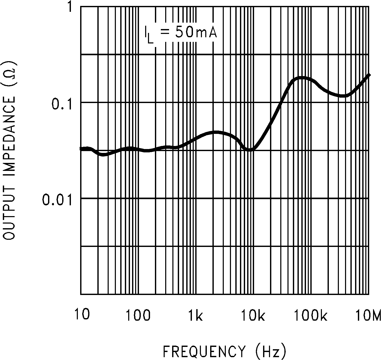 Figure 8. Output Impedance
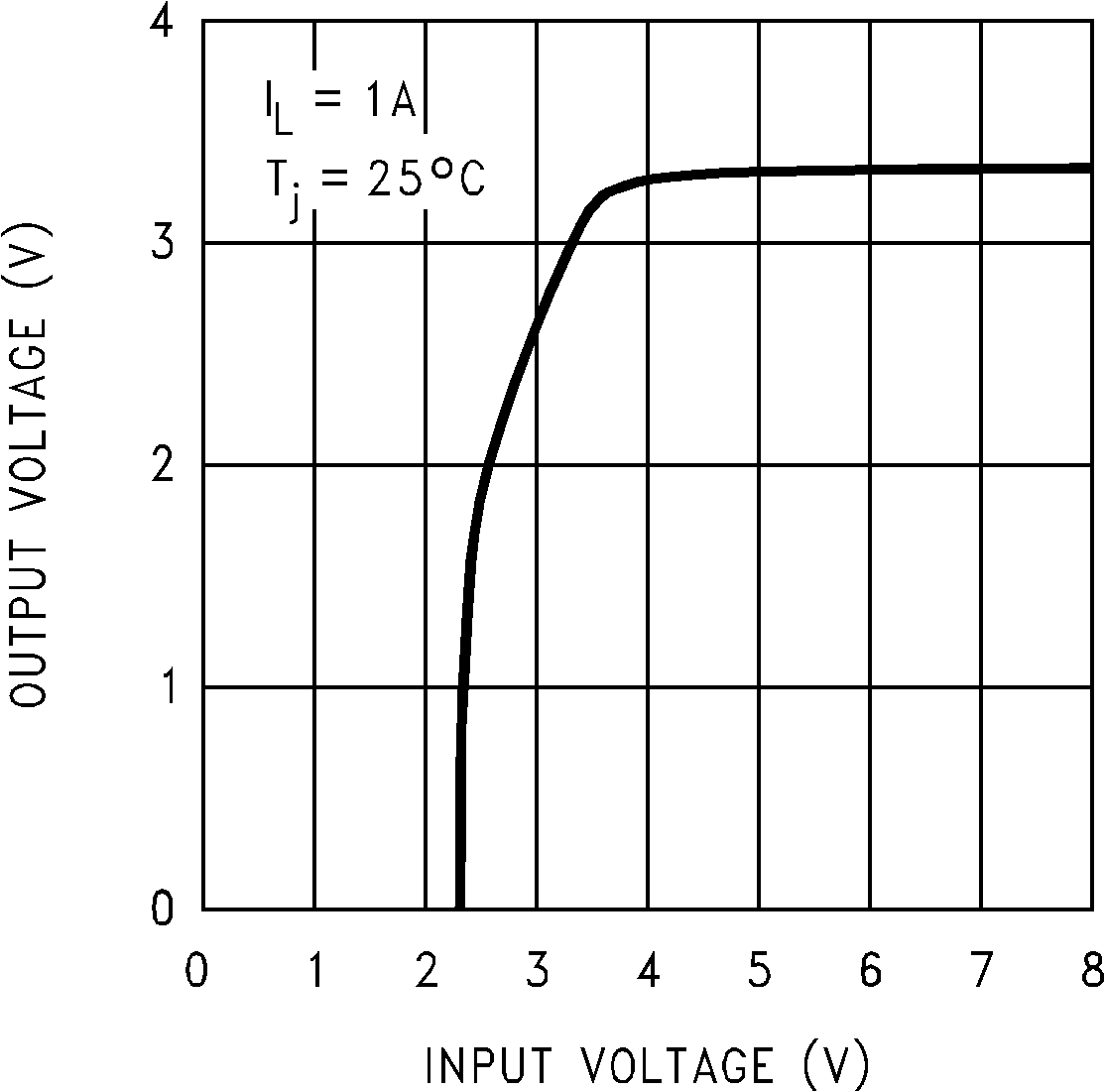 Figure 10. Low Voltage Behavior