SNVS372G August 2005 – October 2016 LM4132 , LM4132-Q1
PRODUCTION DATA.
- 1 Features
- 2 Applications
- 3 Description
- 4 Revision History
- 5 Pin Configuration and Functions
-
6 Specifications
- 6.1 Absolute Maximum Ratings
- 6.2 ESD Ratings
- 6.3 Recommended Operating Conditions
- 6.4 Thermal Information
- 6.5 Electrical Characteristics LM4132-1.8 (VOUT = 1.8 V)
- 6.6 Electrical Characteristics LM4132-2 (VOUT = 2.048 V)
- 6.7 Electrical Characteristics LM4132-2.5 (VOUT = 2.5 V)
- 6.8 Electrical Characteristics LM4132-3 (VOUT = 3 V)
- 6.9 Electrical Characteristics LM4132-3.3 (VOUT = 3.3 V)
- 6.10 Electrical Characteristics LM4132-3.3-Q1(VOUT = 3.3 V)
- 6.11 Electrical Characteristics LM4132-4.1 (VOUT = 4.096 V)
- 6.12 Typical Characteristics
- 7 Detailed Description
- 8 Applications and Implementation
- 9 Power Supply Recommendations
- 10Layout
- 11Device and Documentation Support
- 12Mechanical, Packaging, and Orderable Information
Package Options
Mechanical Data (Package|Pins)
- DBV|5
Thermal pad, mechanical data (Package|Pins)
Orderable Information
8 Applications and Implementation
NOTE
Information in the following applications sections is not part of the TI component specification, and TI does not warrant its accuracy or completeness. TI’s customers are responsible for determining suitability of components for their purposes. Customers should validate and test their design implementation to confirm system functionality.
8.1 Application Information
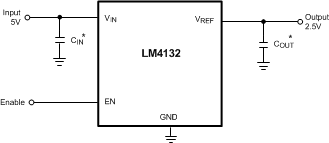
The LM4132 family of precision voltage references can deliver up to 20 mA without an output capacitor or buffer amplifier. The LM4132 is ideal for battery-powered solutions, with a low quiescent current of 60 µA, and a low dropout voltage of 400 mV. The LM4132 enters the shutdown mode (3 µA, typical) when EN is 0 V.
8.2 Typical Applications
8.2.1 LM4132 Typical Application
8.2.1.1 Design Requirements
For this design example, use the parameters listed as the input parameters.
- VIN > VREF + 400 mV (ILOAD ≤ 10 mA)
- ILOAD ≤ 20 mA
- The LM4132 is enabled when 65%VIN< VEN ≤ VIN. VEN cannot be greater than VIN; otherwise, the device does not operate correctly.
- The devices is disabled when 0 V ≤ VEN ≤ 35% VIN.
8.2.1.2 Detailed Design Procedure
The foundation of any voltage reference is the band-gap circuit. While the reference in the LM4132 is developed from the gate-source voltage of transistors in the device, principles of the band-gap circuit are easily understood using a bipolar example. For a detailed analysis of the bipolar band-gap circuit, refer to AN-56 LM113 1.2V Reference (SNVA514).
8.2.1.2.1 Supply and Enable Voltages
To ensure proper operation, VEN and VIN must be within a specified range. An acceptable range of input voltages is calculated by Equation 2:
The EN pin uses an internal pullup current source (IPULLUP ≊ 2 µA) that may be left floating or triggered by an external source. If the device is not enabled by an external source, it may be connected to VIN. An acceptable range of enable voltages is given by Figure 4. See Electrical Characteristics LM4132-1.8 (VOUT = 1.8 V) and Figure 3 for more detail. The device does not operate correctly for VEN > VIN.
8.2.1.2.2 Component Selection
A small ceramic (X5R or X7R) capacitor on the input must be used to ensure stable operation. The value of CIN must be sized according to the output capacitor value. The value of CIN must satisfy the relationship CIN ≥ COUT. When no output capacitor is used, CIN must have a minimum value of 0.1 µF. Noise on the power-supply input may affect the output noise. Larger input capacitor values (typically 4.7 µF to 22 µF) may help reduce noise on the output and significantly reduce overshoot during start-up. Use of an additional optional bypass capacitor from the input and ground may help further reduce noise on the output. With an input capacitor, the LM4132 drives any combination of resistance and capacitance up to VREF / 20 mA and 10 µF, respectively.
The LM4132 is designed to operate with or without an output capacitor and is stable with capacitive loads up to 10 µF. Connecting a capacitor from the output and ground significantly improves the load transient response when switching from a light load to a heavy load. The output capacitor must not be made arbitrarily large because capacitor selection affects the turnon time as well as line and load transients.
While a variety of capacitor chemistry types may be used, it is typically advisable to use low equivalent series resistance (ESR) ceramic capacitors. Such capacitors provide a low impedance to high frequency signals, effectively bypassing them to ground. Bypass capacitors must be mounted close to the device. Mounting bypass capacitors close to the device helps reduce the parasitic trace components thereby improving performance.
8.2.1.2.3 Temperature Coefficient
Temperature drift is defined as the maximum deviation in output voltage over the operating temperature range. This deviation over temperature may be shown in Figure 48:
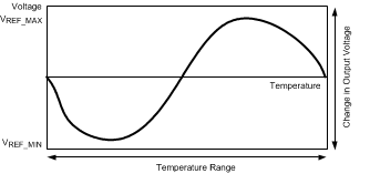 Figure 48. VREF vs Temperature Profile
Temperature coefficient may be expressed analytically as Equation 3:

where
- TD = Temperature drift
- VREF = Nominal preset output voltage
- VREF_MIN = Minimum output voltage over operating temperature range
- VREF_MAX = Maximum output voltage over operating temperature range
- ΔT = Operating temperature range
- The LM4132 features a low temperature drift of 10 ppm (maximum) to 30 ppm (maximum), depending on the grade.
8.2.1.2.4 Long-Term Stability
Long-term stability refers to the fluctuation in output voltage over a long period of time (1000 hours). The LM4132 features a typical long-term stability of 50 ppm over 1000 hours. The measurements are made using 5 units of each voltage option, at a nominal input voltage (5 V), with no load, at room temperature.
8.2.1.2.5 Expression of Electrical Characteristics
Electrical characteristics are typically expressed in mV, ppm, or a percentage of the nominal value. Depending on the application, one expression may be more useful than the other. To convert one quantity to the other one may apply the following:
ppm to mV error in output voltage:

where
- VREF is in volts (V)
- VERROR is in millivolts (mV)
Bit error (1 bit) to voltage error (mV):

where
- VREF is in volts (V)
- VERROR is in millivolts (mV)
- n is the number of bits
mV to ppm error in output voltage:

where
- VREF is in volts (V)
- VERROR is in millivolts (mV)
Voltage error (mV) to percentage error (percent):

where
- VREF is in volts (V)
- VERROR is in millivolts (mV)
8.2.1.3 Application Curves
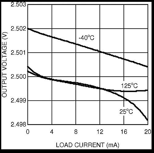 Figure 49. Load Regulation
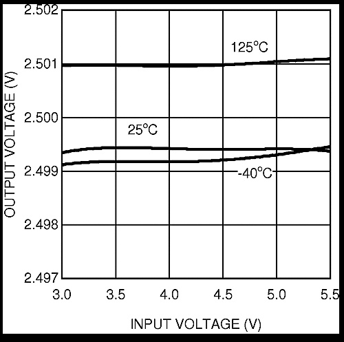 Figure 50. Line Regulation
