SNVS372G August 2005 – October 2016 LM4132 , LM4132-Q1
PRODUCTION DATA.
- 1 Features
- 2 Applications
- 3 Description
- 4 Revision History
- 5 Pin Configuration and Functions
-
6 Specifications
- 6.1 Absolute Maximum Ratings
- 6.2 ESD Ratings
- 6.3 Recommended Operating Conditions
- 6.4 Thermal Information
- 6.5 Electrical Characteristics LM4132-1.8 (VOUT = 1.8 V)
- 6.6 Electrical Characteristics LM4132-2 (VOUT = 2.048 V)
- 6.7 Electrical Characteristics LM4132-2.5 (VOUT = 2.5 V)
- 6.8 Electrical Characteristics LM4132-3 (VOUT = 3 V)
- 6.9 Electrical Characteristics LM4132-3.3 (VOUT = 3.3 V)
- 6.10 Electrical Characteristics LM4132-3.3-Q1(VOUT = 3.3 V)
- 6.11 Electrical Characteristics LM4132-4.1 (VOUT = 4.096 V)
- 6.12 Typical Characteristics
- 7 Detailed Description
- 8 Applications and Implementation
- 9 Power Supply Recommendations
- 10Layout
- 11Device and Documentation Support
- 12Mechanical, Packaging, and Orderable Information
Package Options
Mechanical Data (Package|Pins)
- DBV|5
Thermal pad, mechanical data (Package|Pins)
Orderable Information
6 Specifications
6.1 Absolute Maximum Ratings
over operating free-air temperature range (unless otherwise noted)(1)(2)| MIN | MAX | UNIT | ||
|---|---|---|---|---|
| Voltage | Maximum voltage on any input | –0.3 | 6 | V |
| Output short-circuit duration | Indefinite | |||
| Power dissipation (TA = 25°C)(3) | 350 | mW | ||
| Lead temperature (soldering, 10 sec) | 260 | °C | ||
| Vapor phase (60 sec) | 215 | °C | ||
| Infrared (15 sec) | 220 | °C | ||
| Storage temperature, Tstg | −65 | 150 | °C | |
(1) Stresses beyond those listed under Absolute Maximum Ratings may cause permanent damage to the device. These are stress ratings only, which do not imply functional operation of the device at these or any other conditions beyond those indicated under Recommended Operating Conditions. Exposure to absolute-maximum-rated conditions for extended periods may affect device reliability.
(2) If Military/Aerospace specified devices are required, contact the Texas Instruments Sales Office/Distributors for availability and specifications.
(3) Without PCB copper enhancements. The maximum power dissipation must be de-rated at elevated temperatures and is limited by TJMAX (maximum junction temperature), RθJA (junction to ambient thermal resistance) and TA (ambient temperature). The maximum power dissipation at any temperature is: PDissMAX = (TJMAX – TA) / RθJA up to the value listed in theAbsolute Maximum Ratings. RθJA for SOT-23 is 164.1°C/W, TJMAX = 125°C.
6.2 ESD Ratings
| VALUE | UNIT | |||
|---|---|---|---|---|
| V(ESD) | Electrostatic discharge(1) | Human-body model (HBM), per AEC Q100-002(2) | ±2000 | V |
(1) The Human body model is a 100-pF capacitor discharged through a 1.5-kΩ resistor into each pin.
(2) AEC Q100-002 indicates that HBM stressing shall be in accordance with the ANSI/ESDA/JEDEC JS-001 specification.
6.3 Recommended Operating Conditions
| MIN | NOM | MAX | UNIT | ||
|---|---|---|---|---|---|
| Maximum input supply voltage | 5.5 | V | |||
| Maximum enable input voltage | VIN | V | |||
| Maximum load current | LM4132 | 20 | mA | ||
| LM4132-3.3-Q1 | 25 | mA | |||
| Junction temperature, TJ | –40 | 125 | °C | ||
6.4 Thermal Information
| THERMAL METRIC(1) | LM4132, LM4132-Q1 | UNIT | |
|---|---|---|---|
| DBV (SOT-23) | |||
| 5 PINS | |||
| RθJA | Junction-to-ambient thermal resistance | 164.1 | °C/W |
| RθJC(top) | Junction-to-case (top) thermal resistance | 115.3 | °C/W |
| RθJB | Junction-to-board thermal resistance | 27.1 | °C/W |
| ψJT | Junction-to-top characterization parameter | 12.8 | °C/W |
| ψJB | Junction-to-board characterization parameter | 26.6 | °C/W |
(1) For more information about traditional and new thermal metrics, see the Semiconductor and IC Package Thermal Metrics application report.
6.5 Electrical Characteristics LM4132-1.8 (VOUT = 1.8 V)
Unless otherwise specified, limits are TJ = 25°C, VIN = 5 V, and ILOAD = 0 mA.| PARAMETER | TEST CONDITIONS | MIN(1) | TYP(2) | MAX(1) | UNIT | ||
|---|---|---|---|---|---|---|---|
| VREF | Output voltage initial accuracy | LM4132A-1.8 | (A Grade - 0.05%) | –0.05% | 0.05% | ||
| LM4132B-1.8 | (B Grade - 0.1%) | –0.1% | 0.1% | ||||
| LM4132C-1.8 | (C Grade - 0.2%) | –0.2% | 0.2% | ||||
| LM4132D-1.8 | (D Grade - 0.4%) | –0.4% | 0.4% | ||||
| LM4132E-1.8 | (E Grade - 0.5%) | –0.5% | 0.5% | ||||
| TCVREF/°C | Temperature coefficient | LM4132A-1.8 | 0°C ≤ TJ ≤ 85°C | 10 | ppm/°C | ||
| –40°C ≤ TJ ≤ 125°C | 20 | ||||||
| LM4132B-1.8 | –40°C ≤ TJ ≤ 125°C | 20 | |||||
| LM4132C-1.8 | 20 | ||||||
| LM4132D-1.8 | 20 | ||||||
| LM4132E-1.8 | 30 | ||||||
| IQ | Supply current | 60 | µA | ||||
| –40°C ≤ TJ ≤ 125°C | 100 | ||||||
| IQ_SD | Supply current in shutdown | EN = 0 V | 3 | µA | |||
| –40°C ≤ TJ ≤ 125°C | 7 | ||||||
| ΔVREF/ΔVIN | Line regulation | VREF + 400 mV ≤ VIN ≤ 5.5 V | 30 | ppm/V | |||
| ΔVREF/ΔILOAD | Load regulation | 0 mA ≤ ILOAD ≤ 20 mA | 25 | ppm/mA | |||
| –40°C ≤ TJ ≤ 125°C | 120 | ||||||
| ΔVREF | Long-term stability(3) | 1000 Hrs | 50 | ppm | |||
| Thermal hysteresis(4) | –40°C ≤ TJ ≤ 125°C | 75 | |||||
| VIN – VREF | Dropout voltage(5) | ILOAD = 10 mA | 230 | mV | |||
| –40°C ≤ TJ ≤ 125°C | 400 | ||||||
| VN | Output noise voltage | 0.1 Hz to 10 Hz | 170 | µVPP | |||
| ISC | Short-circuit current | –40°C ≤ TJ ≤ 125°C | 75 | mA | |||
| VIL | Enable pin maximum low input level | –40°C ≤ TJ ≤ 125°C | 35% (VIN) | V | |||
| VIH | Enable pin minimum high input level | –40°C ≤ TJ ≤ 125°C | 65% (VIN) | V | |||
(1) Limits are 100% production tested at 25°C. Limits over the operating temperature range are specified through correlation using Statistical Quality Control.
(2) Typical numbers are at 25°C and represent the most likely parametric norm.
(3) Long-term stability is VREF at 25°C measured during 1000 hrs.
(4) Thermal hysteresis is defined as the change in 25°C output voltage before and after cycling the device from (–40°C to 125°C).
(5) Dropout voltage is defined as the minimum input to output differential at which the output voltage drops by 0.5% below the value measured with a 5-V input.
6.6 Electrical Characteristics LM4132-2 (VOUT = 2.048 V)
Unless otherwise specified, limits are TJ = 25°C, VIN = 5 V, and ILOAD = 0 mA.| PARAMETER | TEST CONDITIONS | MIN(1) | TYP(2) | MAX(1) | UNIT | ||
|---|---|---|---|---|---|---|---|
| VREF | Output voltage initial accuracy | LM4132A-2.0 | (A Grade - 0.05%) | –0.05% | 0.05% | ||
| LM4132B-2.0 | (B Grade - 0.1%) | –0.1% | 0.1% | ||||
| LM4132C-2.0 | (C Grade - 0.2%) | –0.2% | 0.2% | ||||
| LM4132D-2.0 | (D Grade - 0.4%) | –0.4% | 0.4% | ||||
| LM4132E-2.0 | (E Grade - 0.5%) | –0.5% | 0.5% | ||||
| TCVREF/°C | Temperature coefficient | LM4132A-2.0 | 0°C ≤ TJ ≤ 85°C | 10 | ppm/°C | ||
| –40°C ≤ TJ ≤ 125°C | 20 | ||||||
| LM4132B-2.0 | –40°C ≤ TJ ≤ 125°C | 20 | |||||
| LM4132C-2.0 | 20 | ||||||
| LM4132D-2.0 | 20 | ||||||
| LM4132E-2.0 | 30 | ||||||
| IQ | Supply current | 60 | µA | ||||
| –40°C ≤ TJ ≤ 125°C | 100 | ||||||
| IQ_SD | Supply current in shutdown | EN = 0 V | 3 | µA | |||
| –40°C ≤ TJ ≤ 125°C | 7 | ||||||
| ΔVREF/ΔVIN | Line regulation | VREF + 400 mV ≤ VIN ≤ 5.5 V | 30 | ppm/V | |||
| ΔVREF/ΔILOAD | Load regulation | 0 mA ≤ ILOAD ≤ 20 mA | 25 | ppm/mA | |||
| –40°C ≤ TJ ≤ 125°C | 120 | ||||||
| ΔVREF | Long-term stability(3) | 1000 Hrs | 50 | ppm | |||
| Thermal hysteresis(4) | –40°C ≤ TJ ≤ 125°C | 75 | |||||
| VIN – VREF | Dropout voltage(5) | ILOAD = 10 mA | 175 | mV | |||
| –40°C ≤ TJ ≤ 125°C | 400 | ||||||
| VN | Output noise voltage | 0.1 Hz to 10 Hz | 190 | µVPP | |||
| ISC | Short-circuit current | –40°C ≤ TJ ≤ 125°C | 75 | mA | |||
| VIL | Enable pin maximum low input level | –40°C ≤ TJ ≤ 125°C | 35% (VIN) | V | |||
| VIH | Enable pin minimum high input level | –40°C ≤ TJ ≤ 125°C | 65% (VIN) | V | |||
(1) Limits are 100% production tested at 25°C. Limits over the operating temperature range are specified through correlation using Statistical Quality Control.
(2) Typical numbers are at 25°C and represent the most likely parametric norm.
(3) Long-term stability is VREF at 25°C measured during 1000 hrs.
(4) Thermal hysteresis is defined as the change in 25°C output voltage before and after cycling the device from (–40°C to 125°C).
(5) Dropout voltage is defined as the minimum input to output differential at which the output voltage drops by 0.5% below the value measured with a 5-V input.
6.7 Electrical Characteristics LM4132-2.5 (VOUT = 2.5 V)
Unless otherwise specified, limits are TJ = 25°C, VIN = 5 V, and ILOAD = 0 mA.| PARAMETER | TEST CONDITIONS | MIN(1) | TYP(2) | MAX(1) | UNIT | ||
|---|---|---|---|---|---|---|---|
| VREF | Output voltage initial accuracy | LM4132A-2.5 | (A Grade - 0.05%) | –0.05% | 0.05% | ||
| LM4132B-2.5 | (B Grade - 0.1%) | –0.1% | 0.1% | ||||
| LM4132C-2.5 | (C Grade - 0.2%) | –0.2% | 0.2% | ||||
| LM4132D-2.5 | (D Grade - 0.4%) | –0.4% | 0.4% | ||||
| LM4132E-2.5 | (E Grade - 0.5%) | –0.5% | 0.5% | ||||
| TCVREF/°C | Temperature coefficient | LM4132A-2.5 | 0°C ≤ TJ ≤ 85°C | 10 | ppm/°C | ||
| –40°C ≤ TJ ≤ 125°C | 20 | ||||||
| LM4132B-2.5 | –40°C ≤ TJ ≤ 125°C | 20 | |||||
| LM4132C-2.5 | 20 | ||||||
| LM4132D-2.5 | 20 | ||||||
| LM4132E-2.5 | 30 | ||||||
| IQ | Supply current | 60 | µA | ||||
| –40°C ≤ TJ ≤ 125°C | 100 | ||||||
| IQ_SD | Supply current in shutdown | EN = 0 V | 3 | µA | |||
| –40°C ≤ TJ ≤ 125°C | 7 | ||||||
| ΔVREF/ΔVIN | Line regulation | VREF + 400 mV ≤ VIN ≤ 5.5 V | 50 | ppm/V | |||
| ΔVREF/ΔILOAD | Load regulation | 0 mA ≤ ILOAD ≤ 20 mA | 25 | ppm/mA | |||
| –40°C ≤ TJ ≤ 125°C | 120 | ||||||
| ΔVREF | Long-term stability(3) | 1000 Hrs | 50 | ppm | |||
| Thermal hysteresis(4) | –40°C ≤ TJ ≤ 125°C | 75 | |||||
| VIN – VREF | Dropout voltage(5) | ILOAD = 10 mA | 175 | mV | |||
| –40°C ≤ TJ ≤ 125°C | 400 | ||||||
| VN | Output noise voltage | 0.1 Hz to 10 Hz | 240 | µVPP | |||
| ISC | Short-circuit current | –40°C ≤ TJ ≤ 125°C | 75 | mA | |||
| VIL | Enable pin maximum low input level | –40°C ≤ TJ ≤ 125°C | 35% (VIN) | V | |||
| VIH | Enable pin minimum high input level | –40°C ≤ TJ ≤ 125°C | 65% (VIN) | V | |||
(1) Limits are 100% production tested at 25°C. Limits over the operating temperature range are specified through correlation using Statistical Quality Control.
(2) Typical numbers are at 25°C and represent the most likely parametric norm.
(3) Long-term stability is VREF at 25°C measured during 1000 hrs.
(4) Thermal hysteresis is defined as the change in 25°C output voltage before and after cycling the device from (–40°C to 125°C).
(5) Dropout voltage is defined as the minimum input to output differential at which the output voltage drops by 0.5% below the value measured with a 5-V input.
6.8 Electrical Characteristics LM4132-3 (VOUT = 3 V)
Unless otherwise specified, limits are TJ = 25°C, VIN = 5 V, and ILOAD = 0 mA.| PARAMETER | TEST CONDITIONS | MIN(1) | TYP(2) | MAX(1) | UNIT | ||
|---|---|---|---|---|---|---|---|
| VREF | Output voltage initial accuracy | LM4132A-3.0 | (A Grade - 0.05%) | –0.05% | 0.05% | ||
| LM4132B-3.0 | (B Grade - 0.1%) | –0.1% | 0.1% | ||||
| LM4132C-3.0 | (C Grade - 0.2%) | –0.2% | 0.2% | ||||
| LM4132D-3.0 | (D Grade - 0.4%) | –0.4% | 0.4% | ||||
| LM4132E-3.0 | (E Grade - 0.5%) | –0.5% | 0.5% | ||||
| TCVREF/°C | Temperature coefficient | LM4132A-3.0 | 0°C ≤ TJ ≤ 85°C | 10 | ppm/°C | ||
| –40°C ≤ TJ ≤ 125°C | 20 | ||||||
| LM4132B-3.0 | –40°C ≤ TJ ≤ 125°C | 20 | |||||
| LM4132C-3.0 | 20 | ||||||
| LM4132D-3.0 | 20 | ||||||
| LM4132E-3.0 | 30 | ||||||
| IQ | Supply current | 60 | µA | ||||
| –40°C ≤ TJ ≤ 125°C | 100 | ||||||
| IQ_SD | Supply current in shutdown | EN = 0 V | 3 | µA | |||
| –40°C ≤ TJ ≤ 125°C | 7 | ||||||
| ΔVREF/ΔVIN | Line regulation | VREF + 400 mV ≤ VIN ≤ 5.5 V | 70 | ppm/V | |||
| ΔVREF/ΔILOAD | Load regulation | 0 mA ≤ ILOAD ≤ 20 mA | 25 | ppm/mA | |||
| –40°C ≤ TJ ≤ 125°C | 120 | ||||||
| ΔVREF | Long-term stability(3) | 1000 Hrs | 50 | ppm | |||
| Thermal hysteresis(4) | –40°C ≤ TJ ≤ 125°C | 75 | |||||
| VIN – VREF | Dropout voltage(5) | ILOAD = 10 mA | 175 | mV | |||
| –40°C ≤ TJ ≤ 125°C | 400 | ||||||
| VN | Output noise voltage | 0.1 Hz to 10 Hz | 285 | µVPP | |||
| ISC | Short-circuit current | –40°C ≤ TJ ≤ 125°C | 75 | mA | |||
| VIL | Enable pin maximum low input level | –40°C ≤ TJ ≤ 125°C | 35% (VIN) | V | |||
| VIH | Enable pin minimum high input level | –40°C ≤ TJ ≤ 125°C | 65% (VIN) | V | |||
(1) Limits are 100% production tested at 25°C. Limits over the operating temperature range are specified through correlation using Statistical Quality Control.
(2) Typical numbers are at 25°C and represent the most likely parametric norm.
(3) Long-term stability is VREF at 25°C measured during 1000 hrs.
(4) Thermal hysteresis is defined as the change in 25°C output voltage before and after cycling the device from (–40°C to 125°C).
(5) Dropout voltage is defined as the minimum input to output differential at which the output voltage drops by 0.5% below the value measured with a 5-V input.
6.9 Electrical Characteristics LM4132-3.3 (VOUT = 3.3 V)
Unless otherwise specified, limits are TJ = 25°C, VIN = 5 V, and ILOAD = 0 mA.| PARAMETER | TEST CONDITIONS | MIN(1) | TYP(2) | MAX(1) | UNIT | ||
|---|---|---|---|---|---|---|---|
| VREF | Output voltage initial accuracy | LM4132A-3.3 | (A Grade - 0.05%) | –0.05% | 0.05% | ||
| LM4132B-3.3 | (B Grade - 0.1%) | –0.1% | 0.1% | ||||
| LM4132C-3.3 | (C Grade - 0.2%) | –0.2% | 0.2% | ||||
| LM4132D-3.3 | (D Grade - 0.4%) | –0.4% | 0.4% | ||||
| LM4132E-3.3 | (E Grade - 0.5%) | –0.5% | 0.5% | ||||
| TCVREF/°C | Temperature coefficient | LM4132A-3.3 | 0°C ≤ TJ ≤ 85°C | 10 | ppm/°C | ||
| –40°C ≤ TJ ≤ 125°C | 20 | ||||||
| LM4132B-3.3 | –40°C ≤ TJ ≤ 125°C | 20 | |||||
| LM4132C-3.3 | 20 | ||||||
| LM4132D-3.3 | 20 | ||||||
| LM4132E-3.3 | 30 | ||||||
| IQ | Supply current | 60 | µA | ||||
| –40°C ≤ TJ ≤ 125°C | 100 | ||||||
| IQ_SD | Supply current in shutdown | EN = 0 V | 3 | µA | |||
| –40°C ≤ TJ ≤ 125°C | 7 | ||||||
| ΔVREF/ΔVIN | Line regulation | VREF + 400 mV ≤ VIN ≤ 5.5 V | 85 | ppm/V | |||
| ΔVREF/ΔILOAD | Load Regulation | 0 mA ≤ ILOAD ≤ 20 mA | 25 | ppm/mA | |||
| –40°C ≤ TJ ≤ 125°C | 120 | ||||||
| ΔVREF | Long-term stability(3) | 1000 Hrs | 50 | ppm | |||
| Thermal hysteresis(4) | –40°C ≤ TJ ≤ 125°C | 75 | |||||
| VIN – VREF | Dropout voltage(5) | ILOAD = 10 mA | 175 | mV | |||
| –40°C ≤ TJ ≤ 125°C | 400 | ||||||
| VN | Output noise voltage | 0.1 Hz to 10 Hz | 310 | µVPP | |||
| ISC | Short-circuit current | –40°C ≤ TJ ≤ 125°C | 75 | mA | |||
| VIL | Enable pin maximum low input level | –40°C ≤ TJ ≤ 125°C | 35% (VIN) | V | |||
| VIH | Enable pin minimum high input level | –40°C ≤ TJ ≤ 125°C | 65% (VIN) | V | |||
(1) Limits are 100% production tested at 25°C. Limits over the operating temperature range are specified through correlation using Statistical Quality Control.
(2) Typical numbers are at 25°C and represent the most likely parametric norm.
(3) Long-term stability is VREF at 25°C measured during 1000 hrs.
(4) Thermal hysteresis is defined as the change in 25°C output voltage before and after cycling the device from (–40°C to 125°C).
(5) Dropout voltage is defined as the minimum input to output differential at which the output voltage drops by 0.5% below the value measured with a 5-V input.
6.10 Electrical Characteristics LM4132-3.3-Q1(VOUT = 3.3 V)
Unless otherwise specified, limits are TJ = 25°C, VIN = 5 V, and ILOAD = 0 mA.| PARAMETER | TEST CONDITIONS | MIN(1) | TYP(2) | MAX(1) | UNIT | ||
|---|---|---|---|---|---|---|---|
| VREF | Output voltage initial accuracy | LM4132C-3.3-Q1 | (C Grade - 0.2%) | –0.2% | 0.2% | ||
| LM4132D-3.3-Q1 | (D Grade - 0.4%) | –0.4% | 0.4% | ||||
| TCVREF/°C | Temperature coefficient | LM4132C-3.3-Q1 | –40°C ≤ TJ ≤ 125°C | 20 | ppm/°C | ||
| LM4132D-3.3-Q1 | 20 | ||||||
| IQ | Supply current | 60 | µA | ||||
| –40°C ≤ TJ ≤ 125°C | 100 | ||||||
| IQ_SD | Supply current in shutdown | EN = 0 V | 3 | µA | |||
| –40°C ≤ TJ ≤ 125°C | 7 | ||||||
| ΔVREF/ΔVIN | Line regulation | VREF + 400 mV ≤ VIN ≤ 5.5 V | 85 | ppm/V | |||
| ΔVREF/ΔILOAD | Load Regulation | 0 mA ≤ ILOAD ≤ 25 mA | 25 | ppm/mA | |||
| –40°C ≤ TJ ≤ 125°C | 120 | ||||||
| ΔVREF | Long-term stability(3) | 1000 Hrs | 50 | ppm | |||
| Thermal hysteresis(4) | –40°C ≤ TJ ≤ 125°C | 75 | |||||
| VIN – VREF | Dropout voltage(5) | ILOAD = 10 mA | 175 | mV | |||
| –40°C ≤ TJ ≤ 125°C | 400 | ||||||
| VN | Output noise voltage | 0.1 Hz to 10 Hz | 310 | µVPP | |||
| ISC | Short-circuit current | –40°C ≤ TJ ≤ 125°C | 75 | mA | |||
| VIL | Enable pin maximum low input level | –40°C ≤ TJ ≤ 125°C | 35% (VIN) | V | |||
| VIH | Enable pin minimum high input level | –40°C ≤ TJ ≤ 125°C | 65% (VIN) | V | |||
(1) Limits are 100% production tested at 25°C. Limits over the operating temperature range are specified through correlation using Statistical Quality Control.
(2) Typical numbers are at 25°C and represent the most likely parametric norm.
(3) Long-term stability is VREF at 25°C measured during 1000 hrs.
(4) Thermal hysteresis is defined as the change in 25°C output voltage before and after cycling the device from (–40°C to 125°C).
(5) Dropout voltage is defined as the minimum input to output differential at which the output voltage drops by 0.5% below the value measured with a 5-V input.
6.11 Electrical Characteristics LM4132-4.1 (VOUT = 4.096 V)
Unless otherwise specified, limits are TJ = 25°C, VIN = 5 V, and ILOAD = 0 mA.| PARAMETER | TEST CONDITIONS | MIN(1) | TYP(2) | MAX(1) | UNIT | ||
|---|---|---|---|---|---|---|---|
| VREF | Output voltage initial accuracy | LM4132A-4.1 | (A Grade - 0.05%) | –0.05% | 0.05% | ||
| LM4132B-4.1 | (B Grade - 0.1%) | –0.1% | 0.1% | ||||
| LM4132C-4.1 | (C Grade - 0.2%) | –0.2% | 0.2% | ||||
| LM4132D-4.1 | (D Grade - 0.4%) | –0.4% | 0.4% | ||||
| LM4132E-4.1 | (E Grade - 0.5%) | –0.5% | 0.5% | ||||
| TCVREF/°C | Temperature coefficient | LM4132A-4.1 | 0°C ≤ TJ ≤ 85°C | 10 | ppm/°C | ||
| –40°C ≤ TJ ≤ 125°C | 20 | ||||||
| LM4132B-4.1 | –40°C ≤ TJ ≤ 125°C | 20 | |||||
| LM4132C-4.1 | 20 | ||||||
| LM4132D-4.1 | 20 | ||||||
| LM4132E-4.1 | 30 | ||||||
| IQ | Supply current | 60 | µA | ||||
| –40°C ≤ TJ ≤ 125°C | 100 | ||||||
| IQ_SD | Supply current in shutdown | EN = 0 V | 3 | µA | |||
| –40°C ≤ TJ ≤ 125°C | 7 | ||||||
| ΔVREF/ΔVIN | Line regulation | VREF + 400 mV ≤ VIN ≤ 5.5 V | 100 | ppm/V | |||
| ΔVREF/ΔILOAD | Load regulation | 0 mA ≤ ILOAD ≤ 20 mA | 25 | ppm/mA | |||
| –40°C ≤ TJ ≤ 125°C | 120 | ||||||
| ΔVREF | Long-term stability(3) | 1000 Hrs | 50 | ppm | |||
| Thermal hysteresis(4) | –40°C ≤ TJ ≤ 125°C | 75 | |||||
| VIN – VREF | Dropout voltage(5) | ILOAD = 10 mA | 175 | mV | |||
| –40°C ≤ TJ ≤ 125°C | 400 | ||||||
| VN | Output noise voltage | 0.1 Hz to 10 Hz | 350 | µVPP | |||
| ISC | Short-circuit current | –40°C ≤ TJ ≤ 125°C | 75 | mA | |||
| VIL | Enable pin maximum low input level | –40°C ≤ TJ ≤ 125°C | 35% (VIN) | V | |||
| VIH | Enable pin minimum high input level | –40°C ≤ TJ ≤ 125°C | 65% (VIN) | V | |||
(1) Limits are 100% production tested at 25°C. Limits over the operating temperature range are specified through correlation using Statistical Quality Control.
(2) Typical numbers are at 25°C and represent the most likely parametric norm.
(3) Long-term stability is VREF at 25°C measured during 1000 hrs.
(4) Thermal hysteresis is defined as the change in 25°C output voltage before and after cycling the device from (–40°C to 125°C).
(5) Dropout voltage is defined as the minimum input to output differential at which the output voltage drops by 0.5% below the value measured with a 5-V input.
6.12 Typical Characteristics
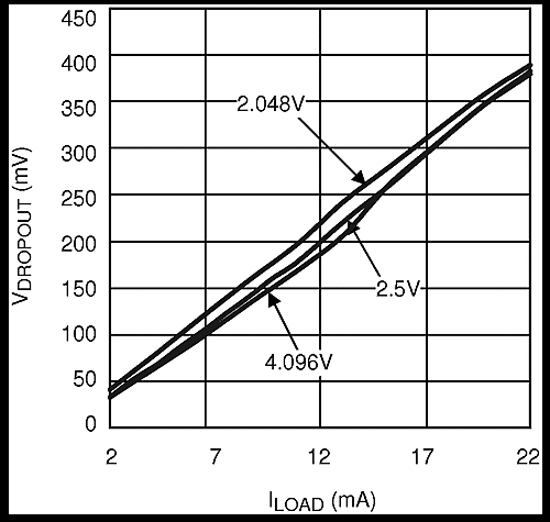 Figure 1. Dropout vs Load to 0.5% Accuracy
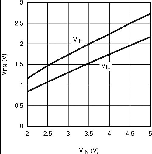 Figure 3. Enable Threshold Voltage and Hysteresis
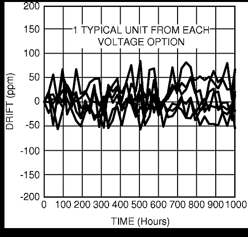 Figure 5. Typical Long-Term Stability
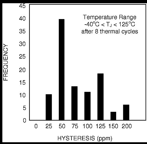 Figure 7. Typical Thermal Hysteresis
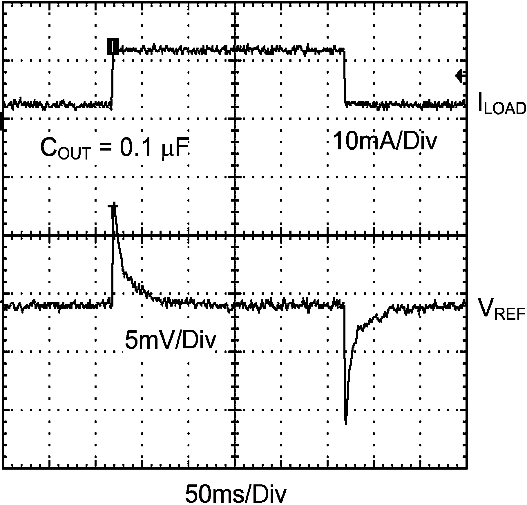
| ILOAD = 0 to 10 mA |
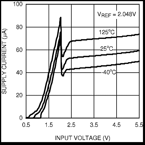 Figure 2. Supply Current vs Input Voltage
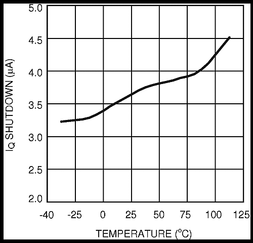 Figure 4. Shutdown IQ vs Temperature
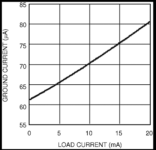 Figure 6. Ground Current vs Load Current
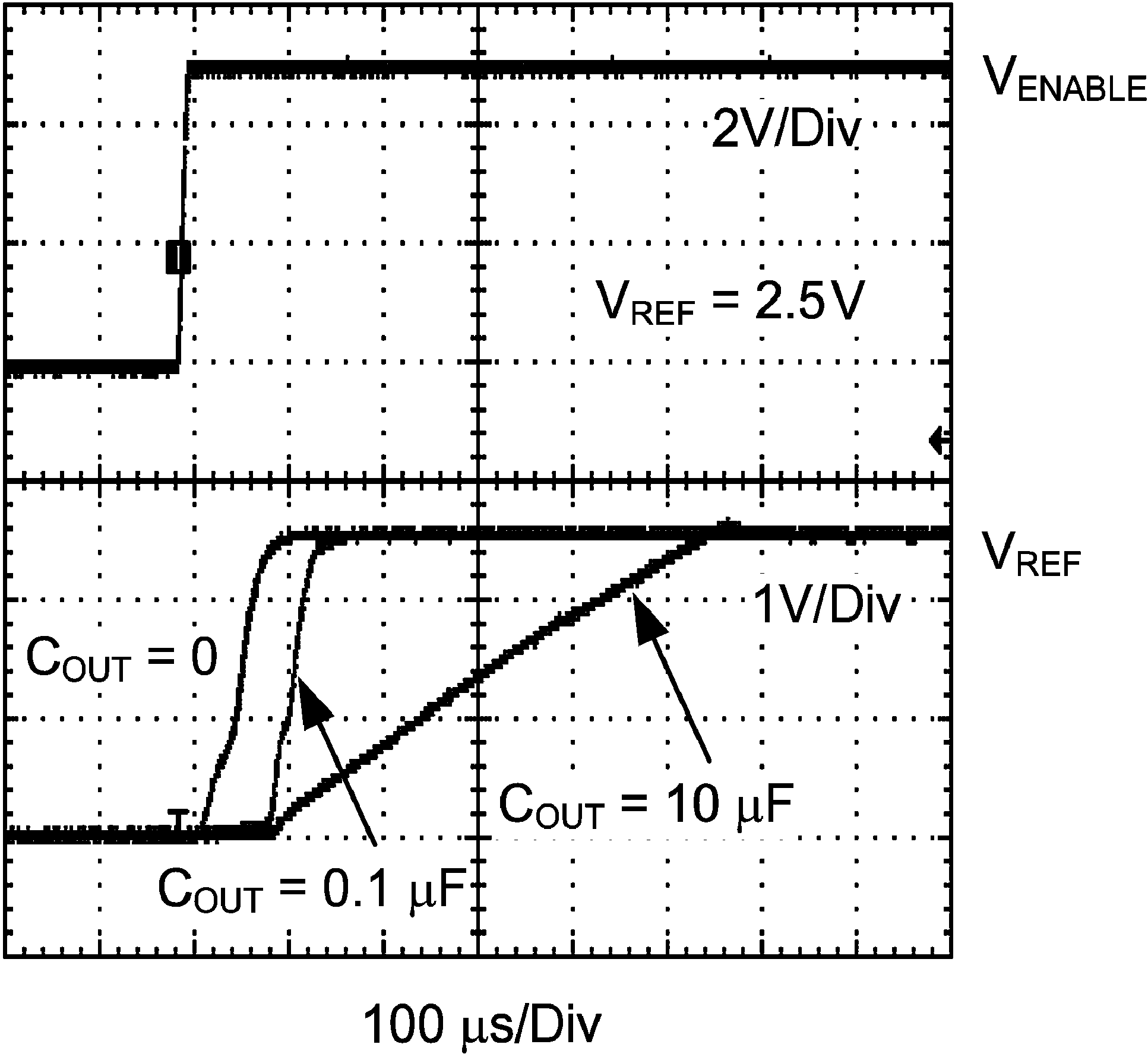 Figure 8. Turnon Transient Response
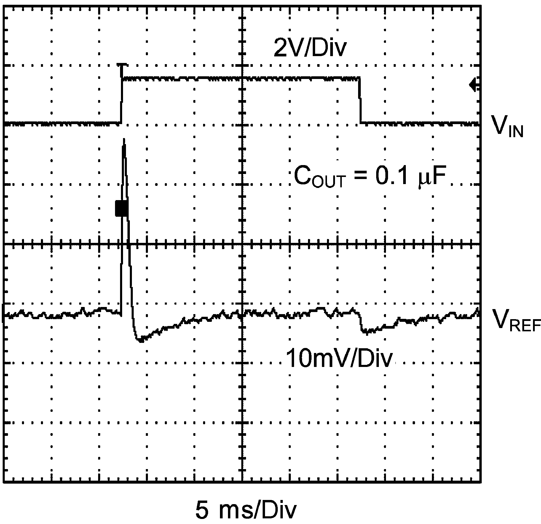
| VIN = 4 V to 5.5 V |
6.12.1 Typical Characteristics for 1.8 V
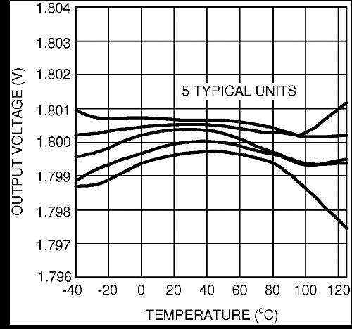 Figure 11. Output Voltage vs Temperature
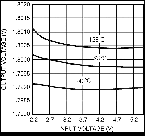 Figure 13. Line Regulation
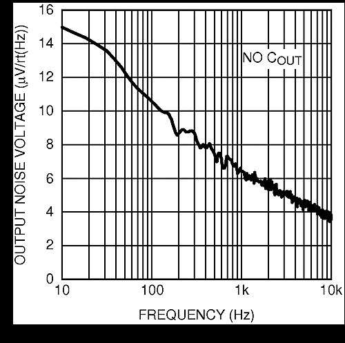 Figure 15. Output Voltage Noise Spectrum
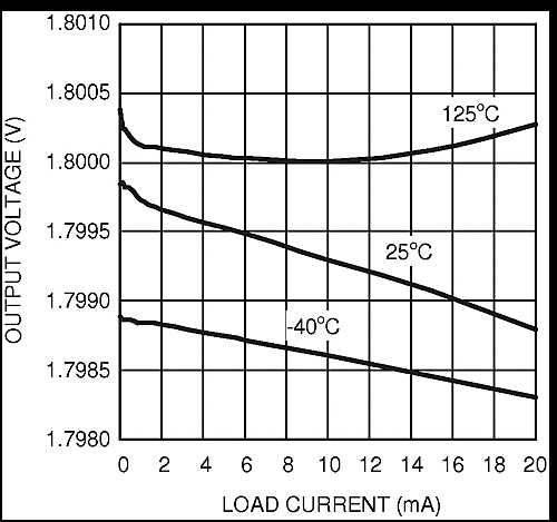 Figure 12. Load Regulation
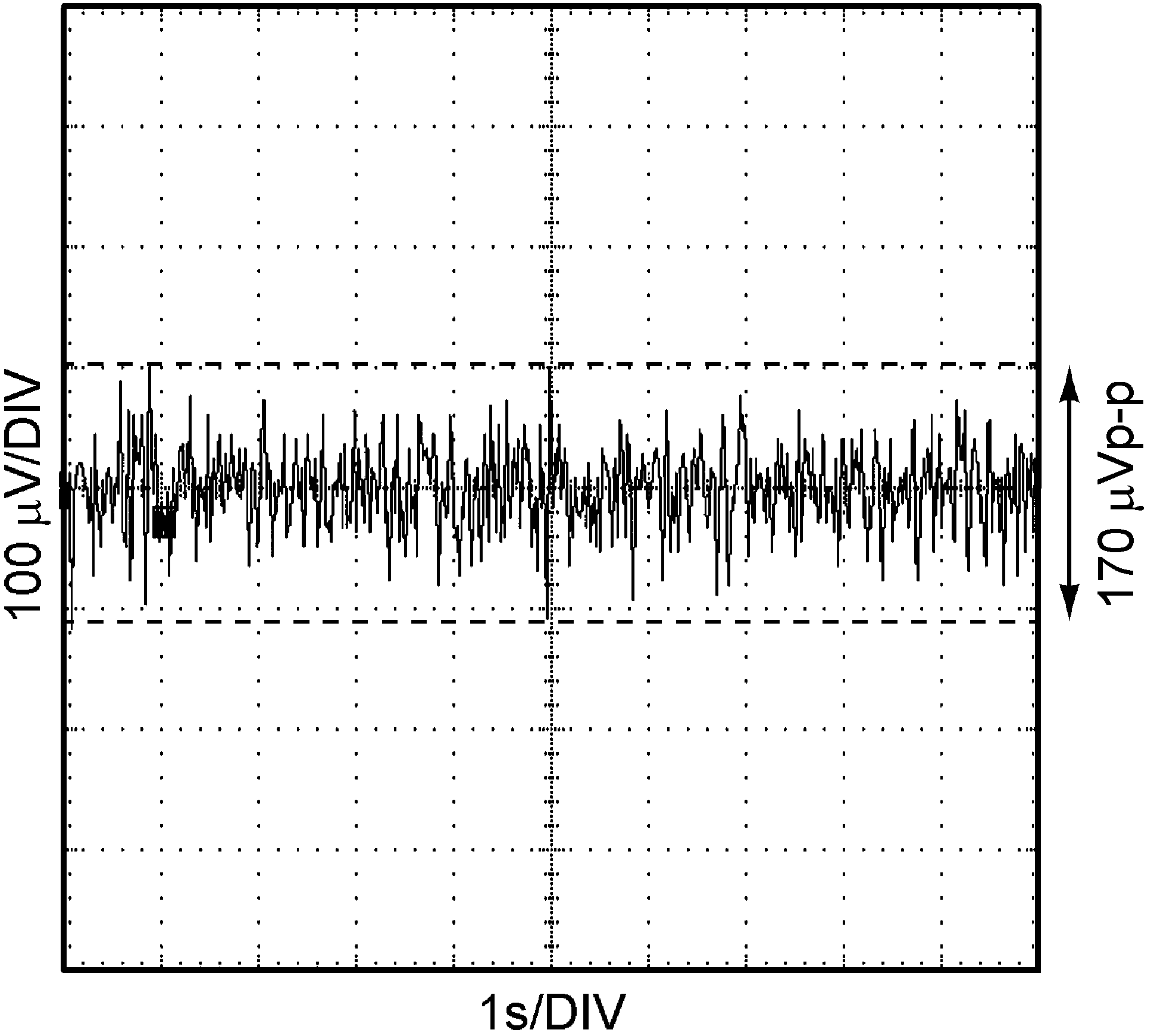 Figure 14. 0.1–10 Hz Noise
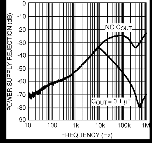 Figure 16. Power Supply Rejection vs Frequency
6.12.2 Typical Characteristics for 2.048 V
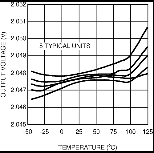 Figure 17. Output Voltage vs Temperature
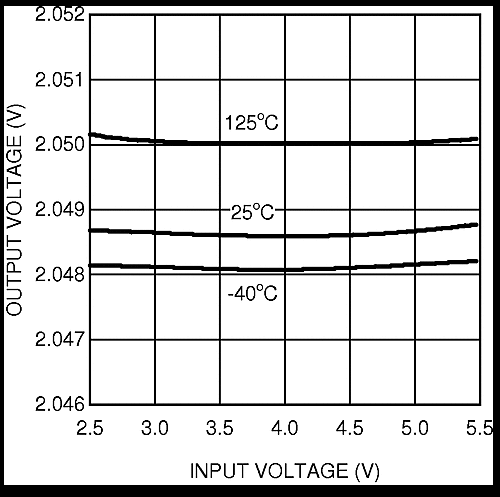 Figure 19. Line Regulation
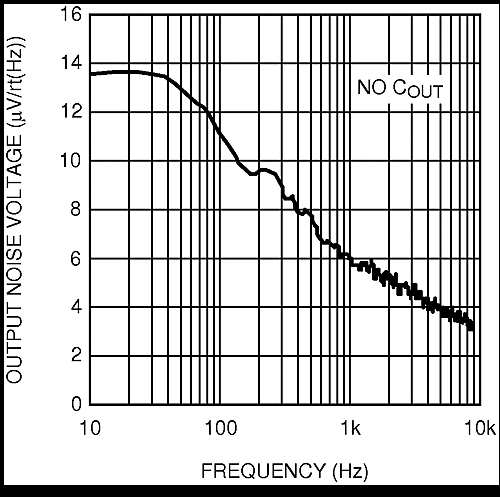 Figure 21. Output Voltage Noise Spectrum
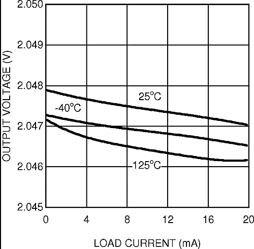 Figure 18. Load Regulation
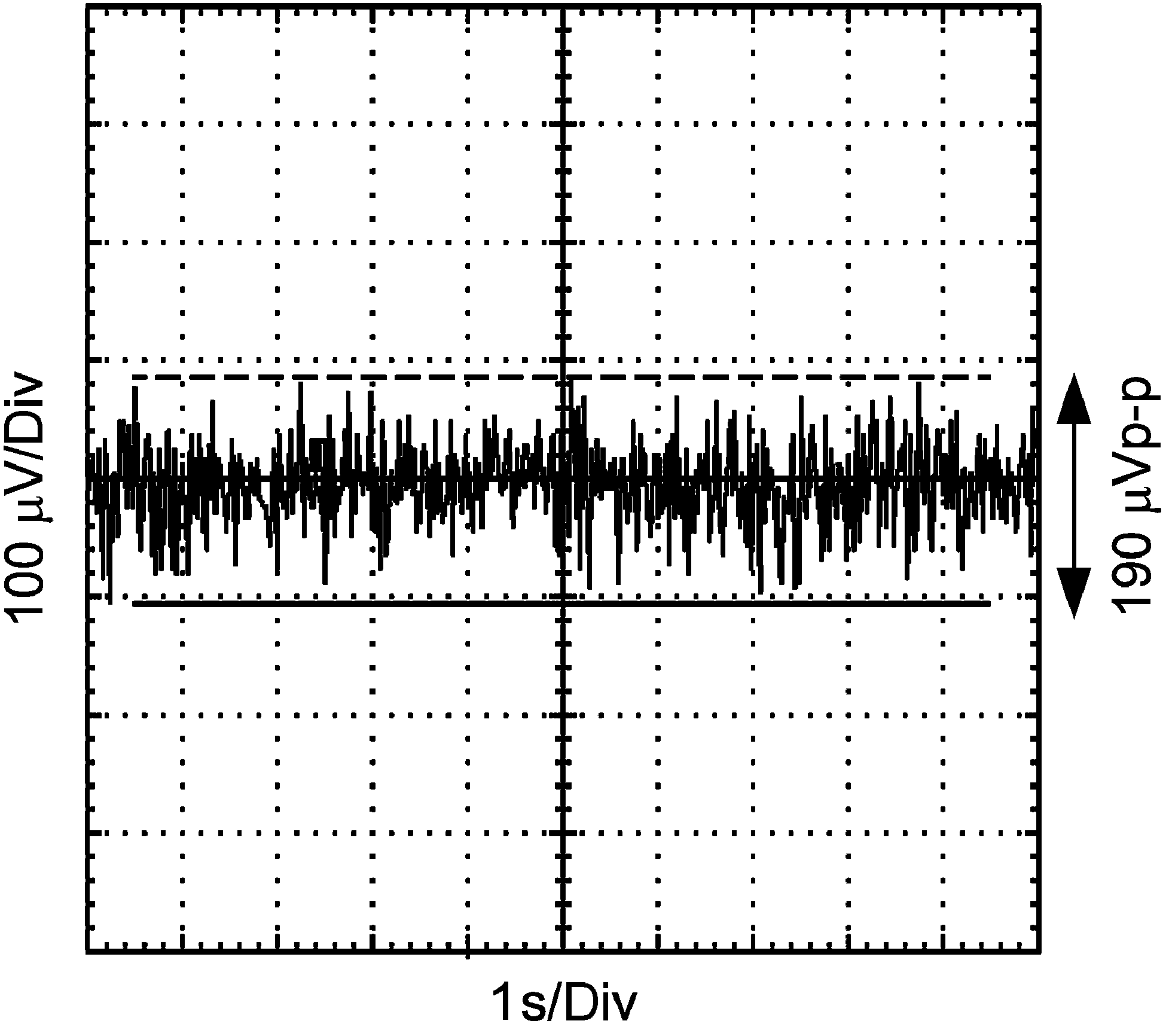 Figure 20. 0.1–10 Hz Noise
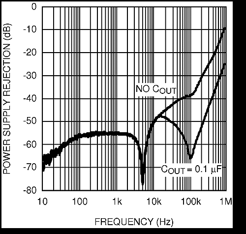 Figure 22. Power Supply Rejection vs Frequency
6.12.3 Typical Characteristics for 2.5 V
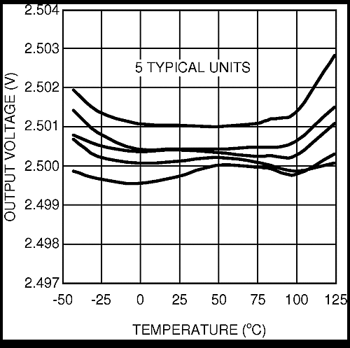 Figure 23. Output Voltage vs Temperature
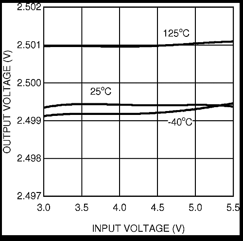 Figure 25. Line Regulation
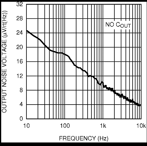 Figure 27. Output Voltage Noise Spectrum
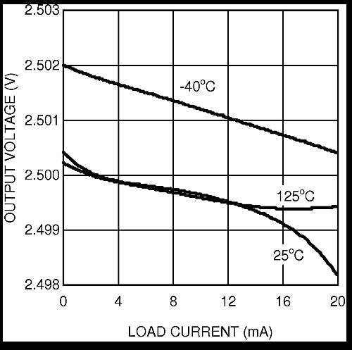 Figure 24. Load Regulation
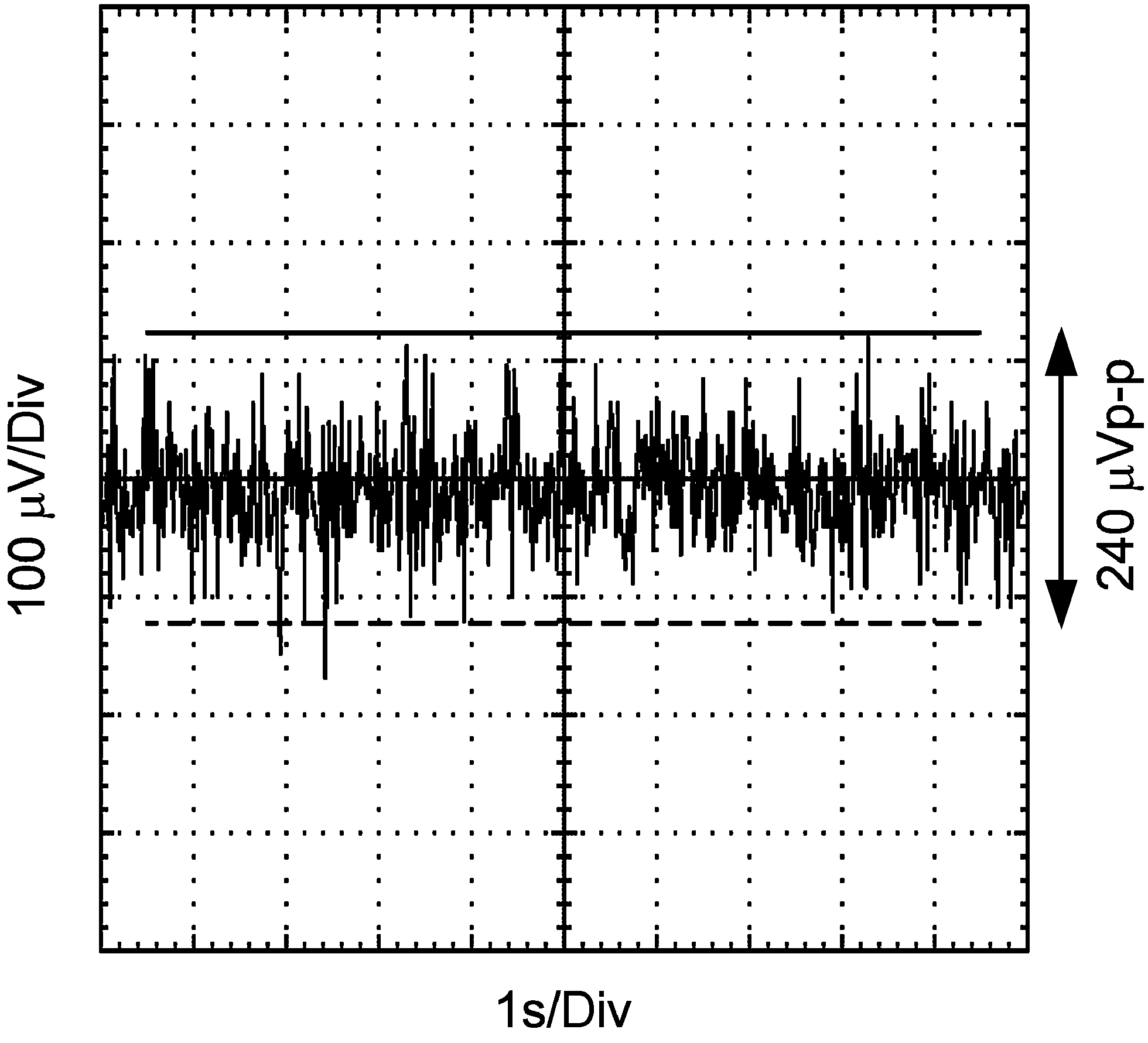 Figure 26. 0.1–10 Hz Noise
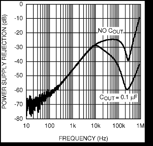 Figure 28. Power Supply Rejection vs Frequency
6.12.4 Typical Characteristics for 3 V
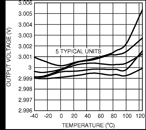 Figure 29. Output Voltage vs Temperature
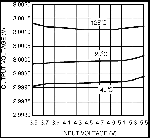 Figure 31. Line Regulation
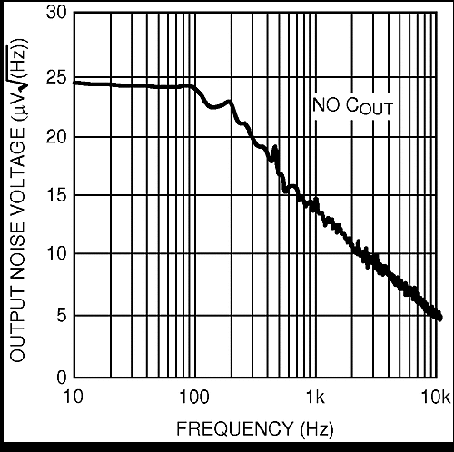 Figure 33. Output Voltage Noise Spectrum
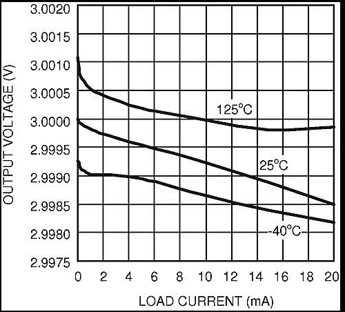 Figure 30. Load Regulation
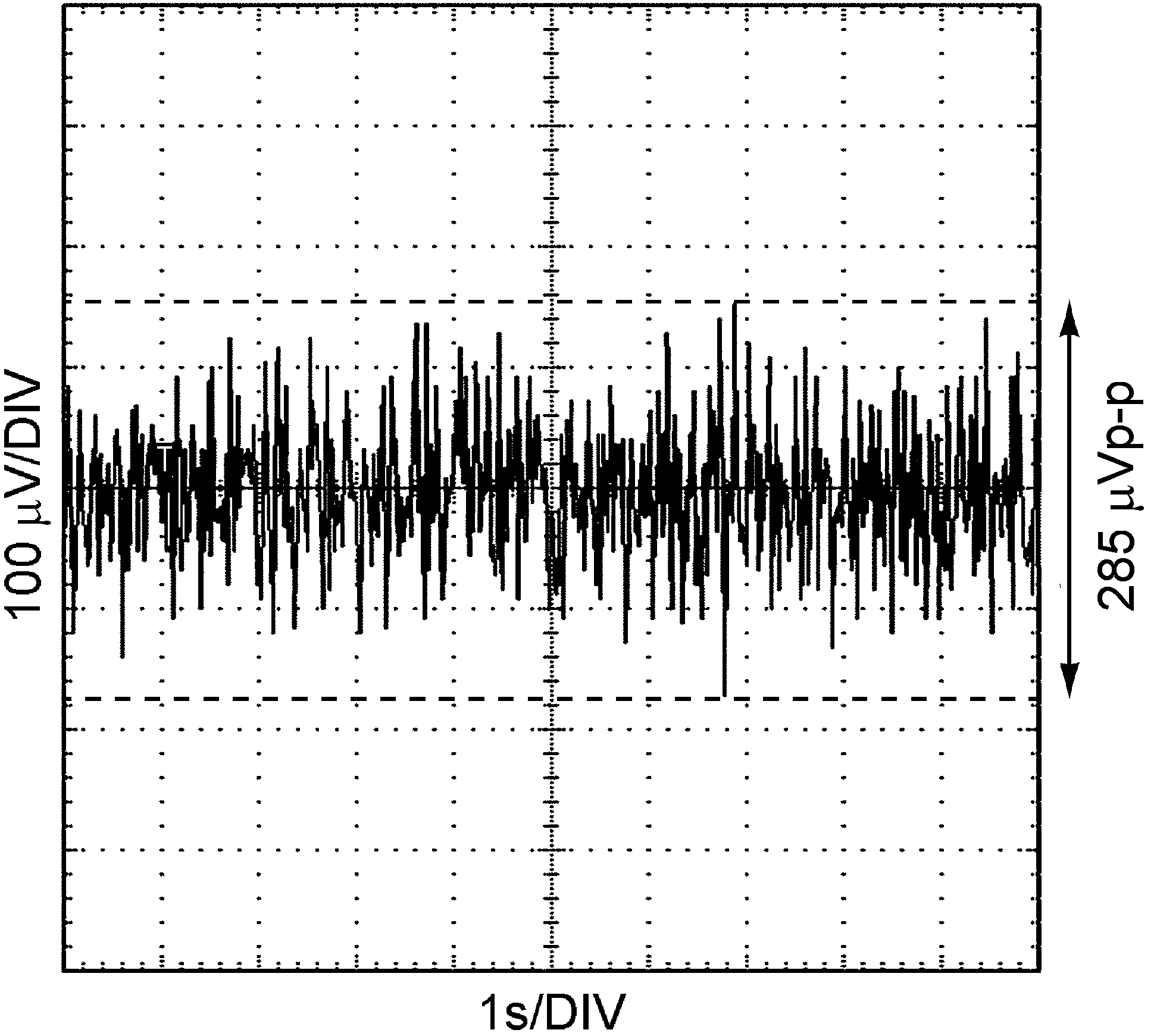 Figure 32. 0.1–10 Hz Noise
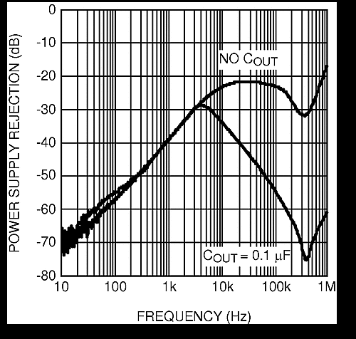 Figure 34. Power Supply Rejection vs Frequency
6.12.5 Typical Characteristics for 3.3 V
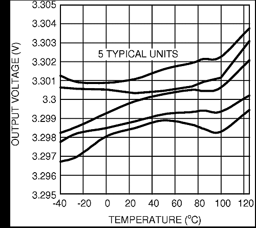 Figure 35. Output Voltage vs Temperature
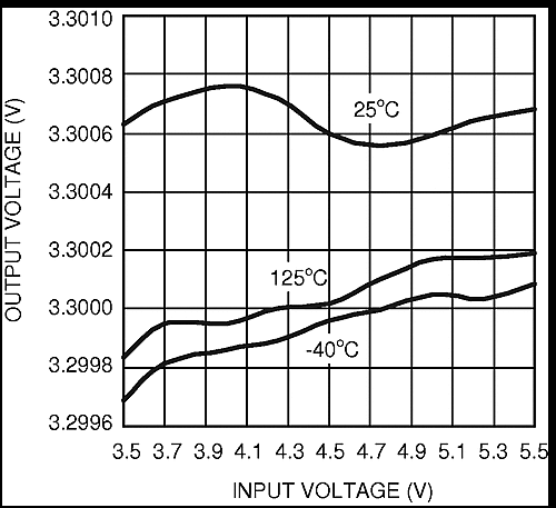 Figure 37. Line Regulation
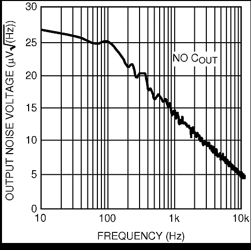 Figure 39. Output Voltage Noise Spectrum
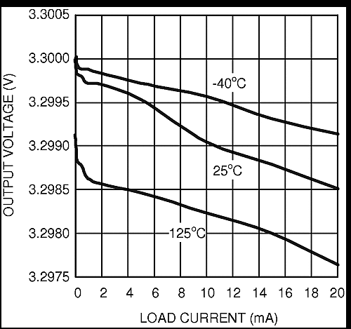 Figure 36. Load Regulation
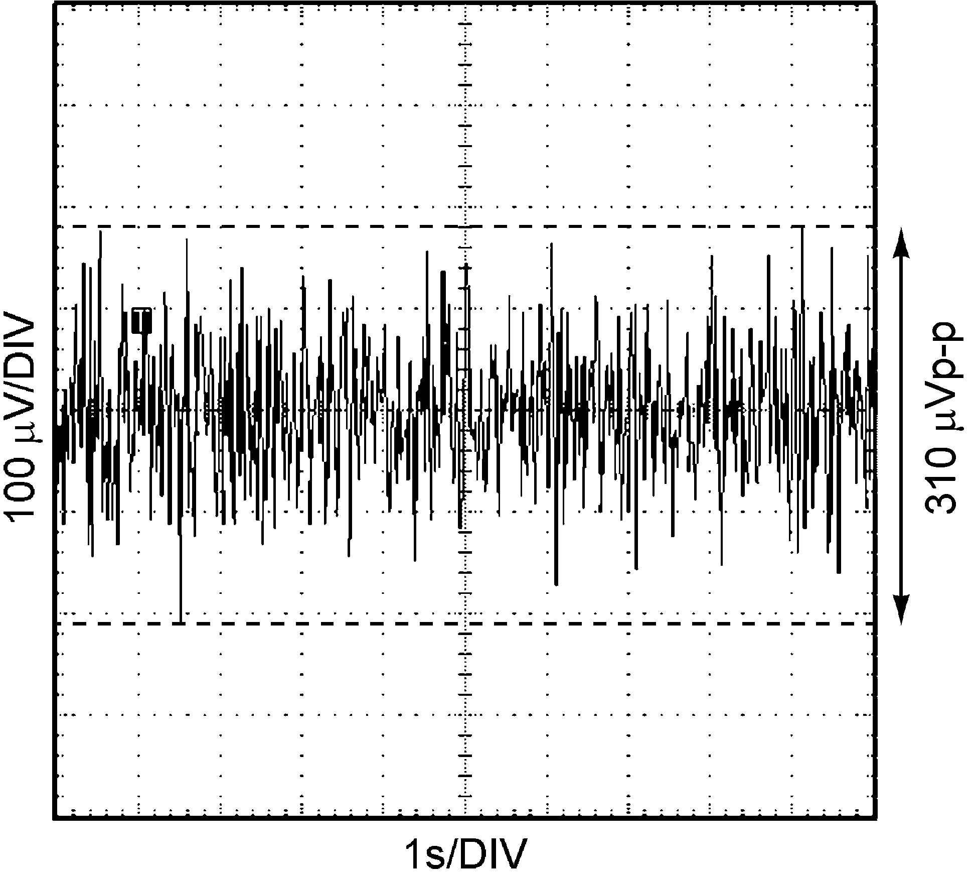 Figure 38. 0.1–10 Hz Noise
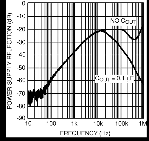 Figure 40. Power Supply Rejection vs Frequency
6.12.6 Typical Characteristics for 4.096 V
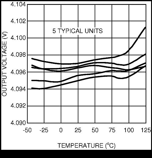 Figure 41. Output Voltage vs Temperature
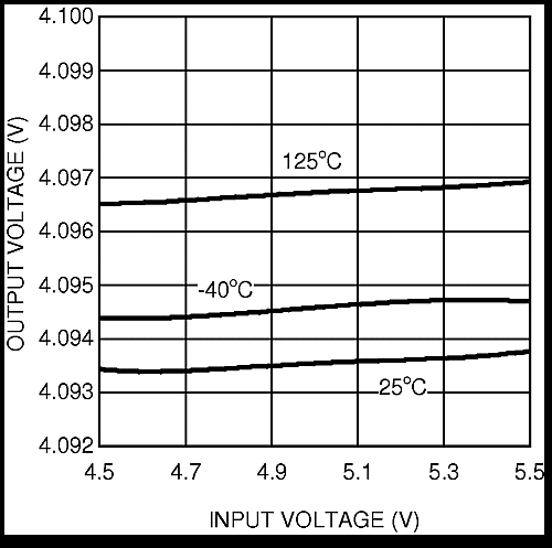 Figure 43. Line Regulation
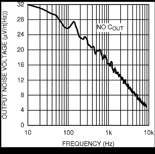 Figure 45. Output Voltage Noise Spectrum
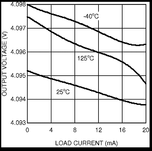 Figure 42. Load Regulation
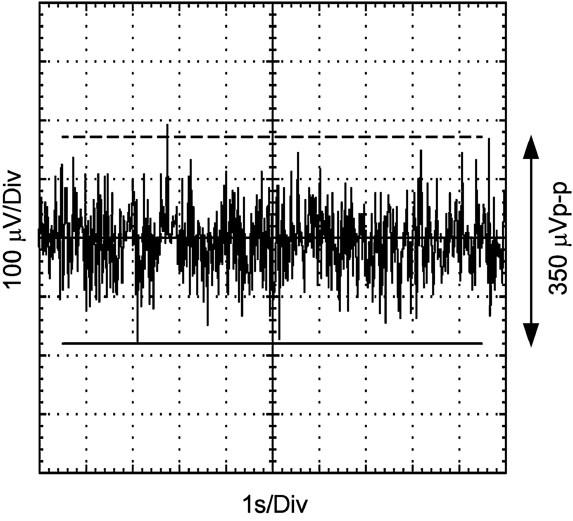 Figure 44. 0.1–10 Hz Noise
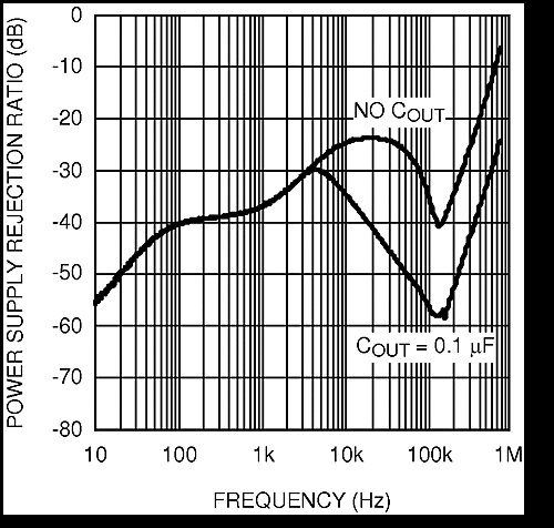 Figure 46. Power Supply Rejection vs Frequency