SNVS783K January 2012 – August 2021 LM5017
PRODUCTION DATA
- 1 Features
- 2 Applications
- 3 Description
- 4 Revision History
- 5 Pin Configuration and Functions
- 6 Specifications
-
7 Detailed Description
- 7.1 Overview
- 7.2 Functional Block Diagram
- 7.3
Feature Description
- 7.3.1 Control Overview
- 7.3.2 VCC Regulator
- 7.3.3 Regulation Comparator
- 7.3.4 Overvoltage Comparator
- 7.3.5 On-Time Generator
- 7.3.6 Current Limit
- 7.3.7 N-Channel Buck Switch and Driver
- 7.3.8 Synchronous Rectifier
- 7.3.9 Undervoltage Detector
- 7.3.10 Thermal Protection
- 7.3.11 Ripple Configuration
- 7.3.12 Soft-Start
- 7.4 Device Functional Modes
-
8 Application and Implementation
- 8.1 Application Information
- 8.2
Typical Application
- 8.2.1 Application Circuit: 12.5-V to 95-V Input and 10-V, 600-mA Output Buck Converter
- 8.2.2
Isolated DC/DC Converter Using LM5017
- 8.2.2.1 Design Requirements
- 8.2.2.2
Detailed Design Procedure
- 8.2.2.2.1 Transformer Turns Ratio
- 8.2.2.2.2 Total IOUT
- 8.2.2.2.3 RFB1, RFB2
- 8.2.2.2.4 Frequency Selection
- 8.2.2.2.5 Transformer Selection
- 8.2.2.2.6 Primary Output Capacitor
- 8.2.2.2.7 Secondary Output Capacitor
- 8.2.2.2.8 Type III Feedback Ripple Circuit
- 8.2.2.2.9 Secondary Diode
- 8.2.2.2.10 VCC and Boostrap Capacitor
- 8.2.2.2.11 Input Capacitor
- 8.2.2.2.12 UVLO Resistors
- 8.2.2.2.13 VCC Diode
- 8.2.2.3 Application Curves
- 9 Power Supply Recommendations
- 10Layout
- 11Device and Documentation Support
- 12Mechanical, Packaging, and Orderable Information
Package Options
Mechanical Data (Package|Pins)
Thermal pad, mechanical data (Package|Pins)
- DDA|8
Orderable Information
8.2.2.2.8 Type III Feedback Ripple Circuit
Type III ripple circuit as described in Section 7.3.11 is required for the Fly-Buck topology. Type I and Type II ripple circuits use series resistance and the triangular inductor ripple current to generate ripple at VOUT and the FB pin. The primary ripple current of a Fly-Buck is the combination or primary and reflected secondary currents as illustrated in Figure 8-6. In the Fly-Buck topology, Type I and Type II ripple circuits suffer from large jitter as the reflected load current affects the feedback ripple.
 Figure 8-8 Type III Ripple Circuit
Selecting the Type III ripple components using the equations from Section 7.3.11 will ensure that the FB pin ripple is be greater than the capacitive ripple from the primary output capacitor COUT1. The feedback ripple component values are chosen as shown in Equation 30.
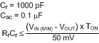
The calculated value for Rr is 66 kΩ. This value provides the minimum ripple for stable operation. A smaller resistance should be selected to allow for variations in TON, COUT1 and other components. For this design, Rr value of 46.4 kΩ is selected.