SNVS293F December 2004 – August 2016 LM5025A
PRODUCTION DATA.
- 1 Features
- 2 Applications
- 3 Description
- 4 Revision History
- 5 Pin Configuration and Functions
- 6 Specifications
- 7 Detailed Description
- 8 Application and Implementation
- 9 Power Supply Recommendations
- 10Layout
- 11Device and Documentation Support
- 12Mechanical, Packaging, and Orderable Information
Package Options
Mechanical Data (Package|Pins)
Thermal pad, mechanical data (Package|Pins)
Orderable Information
7 Detailed Description
7.1 Overview
The LM5025A PWM controller contains all of the features necessary to implement active clamp / reset technique voltage-mode controlled power converters. Synchronous rectification allows higher conversion efficiency and greater power density than conventional PN or Schottky rectifier techniques. The high voltage start-up regulator of the LM5025A can be configured to operate with input voltages ranging from 13 V to 90 V. Additional features include line undervoltage lockout, cycle-by-cycle current limit, voltage feed-forward compensation, hiccup mode fault protection with adjustable delays, soft-start, a 1-MHz capable oscillator with synchronization capability, precision reference, and thermal shutdown. These features simplify the design of active voltage-mode active clamp / reset DC-DC power converters.
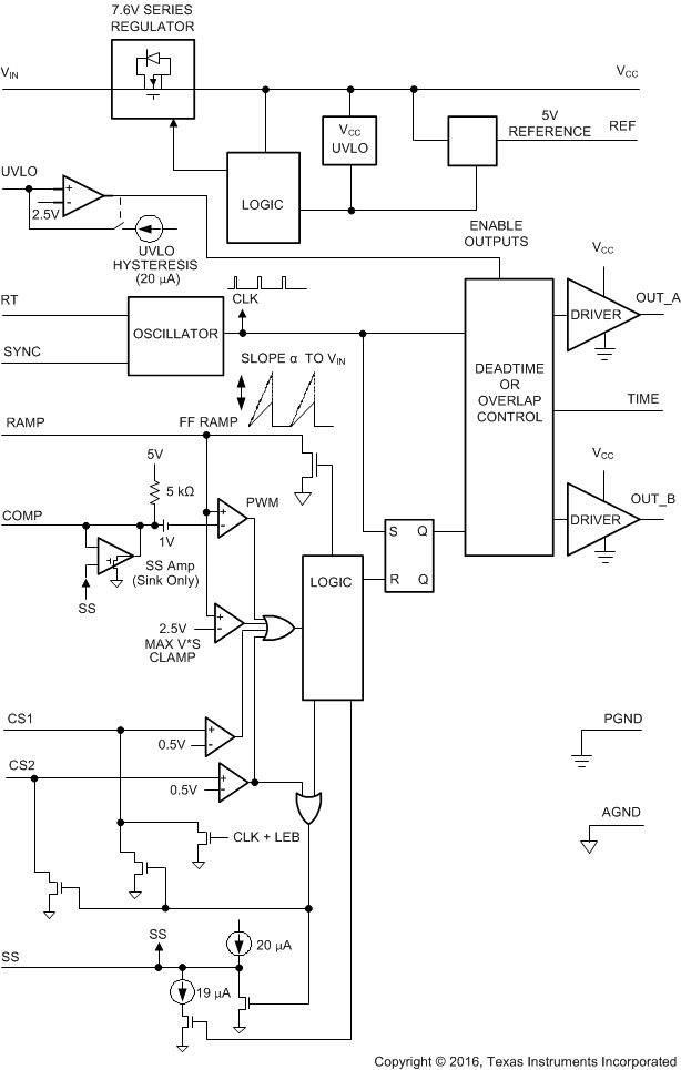
7.2 Functional Block Diagram

7.3 Feature Description
7.3.1 High-Voltage Start-Up Regulator
The LM5025A contains an internal high-voltage start-up regulator that allows the input pin (VIN) to be connected directly to the line voltage. The regulator output is internally current-limited to 20 mA. When power is applied, the regulator is enabled and sources current into an external capacitor connected to the VCC pin. The recommended capacitance range for the VCC regulator is 0.1 µF to 100 µF. When the voltage on the VCC pin reaches the regulation point of 7.6 V and the internal voltage reference (REF) reaches its regulation point of 5 V, the controller outputs are enabled. The outputs remain enabled until VCC falls below 6.2 V or the line undervoltage lockout detector indicates that VIN is out of range. In typical applications, an auxiliary transformer winding is connected through a diode to the VCC pin. This winding must raise the VCC voltage above 8 V to shut off the internal start-up regulator. Powering VCC from an auxiliary winding improves efficiency while reducing the controller power dissipation.
When the converter auxiliary winding is inactive, external current draw on the VCC line must be limited so the power dissipated in the start-up regulator does not exceed the maximum power dissipation of the controller.
An external start-up regulator or other bias rail can be used instead of the internal start-up regulator by connecting the VCC and the VIN pins together and feeding the external bias voltage into the two pins.
7.3.2 Line Undervoltage Detector
The LM5025A contains a line undervoltage lockout (UVLO) circuit. An external setpoint voltage divider from VIN to GND, sets the operational range of the converter. The divider must be designed such that the voltage at the UVLO pin is greater than 2.5 V when VIN is in the desired operating range. If the undervoltage threshold is not met, both outputs are disabled, all other functions of the controller remain active. UVLO hysteresis is accomplished with an internal 20-µA current source that is switched ON or OFF into the impedance of the setpoint divider. When the UVLO threshold is exceeded, the current source is activated to instantly raise the voltage at the UVLO pin. When the UVLO pin voltage falls below the 2.5-V threshold, the current source is turned off, causing the voltage at the UVLO pin to fall. The UVLO pin can also be used to implement a remote enable and disable function. Pulling the UVLO pin below the 2.5-V threshold disables the PWM outputs.
7.3.3 PWM Outputs
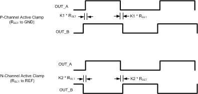
The relative phase of the main (OUT_A) and active clamp outputs (OUT_B) can be configured for the specific application. For active clamp configurations using a ground-referenced P-channel clamp switch, the two outputs must be in-phase with the active clamp output overlapping the main output. For active clamp configurations using a high-side N-channel switch, the active clamp output must be out-of-phase with main output, and there must be a dead time between the two gate drive pulses. A distinguishing feature of the LM5025A is the ability to accurately configure either dead time (both OFF) or overlap time (both ON) of the gate driver outputs. The overlap and dead-time magnitude is controlled by the resistor value connected to the TIME pin of the controller. The opposite end of the resistor can be connected to either REF for dead-time control or GND for overlap control. The internal configuration detector senses the connection and configures the phase relationship of the main and active clamp outputs. The magnitude of the overlap and dead time can be calculated in Equation 1 and Equation 2.
where
- RSET in kΩ
- Time in ns
 Figure 10. PWM Outputs
7.3.4 Compound Gate Drivers
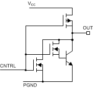
The LM5025A contains two unique compound gate drivers, which parallel both MOS and Bipolar devices to provide high-drive current throughout the entire switching event. The bipolar device provides most of the drive current capability and provides a relatively constant sink current which is ideal for driving large power MOSFETs. As the switching event nears conclusion and the bipolar device saturates, the internal MOS device continues to provide a low impedance to compete the switching event.
During turnoff at the Miller plateau region, typically around 2 V to 3 V, is where gate driver current capability is needed most. The resistive characteristics of all MOS gate drivers are adequate for turnon because the supply to output voltage differential is fairly large at the Miller region. During turnoff however, the voltage differential is small and the current source characteristic of the bipolar gate driver is beneficial to provide fast drive capability.
 Figure 11. Compound Gate Drivers
7.3.5 PWM Comparator
The PWM comparator compares the ramp signal (RAMP) to the loop error signal (COMP). This comparator is optimized for speed to achieve minimum controllable duty cycles. The internal 5-kΩ pullup resistor, connected between the internal 5-V reference and COMP, can be used as the pullup for an optocoupler. The comparator polarity is such that 0 V on the COMP pin produces a zero duty cycle on both gate driver outputs.
7.3.6 Volt Second Clamp
The Volt × Second Clamp comparator compares the ramp signal (RAMP) to a fixed 2.5-V reference. By proper selection of RFF and CFF, the maximum ON-time of the main switch can be set to the desired duration. The ON-time set by Volt × Second Clamp varies inversely with the line voltage because the RAMP capacitor is charged by a resistor connected to VIN while the threshold of the clamp is a fixed voltage (2.5 V). An example illustrates the use of the Volt × Second Clamp comparator to achieve a 50% duty cycle limit, at 200 KHz, at a 48-V line input: A 50% duty cycle at a 200 KHz requires a 2.5 µs of ON-time. At 48-V input the Volt × Second product is 120 V × µs (48 V × 2.5 µs). To achieve this clamp level, use Equation 3 and Equation 4:
Select CFF = 470 pF
RFF = 102 kΩ
The recommended capacitor value range for CFF is 100 pF to 1000 pF.
The CFF ramp capacitor is discharged at the conclusion of every cycle by an internal discharge switch controlled by either the internal clock or by the V × S Clamp comparator, whichever event occurs first.
7.3.7 Current Limit
The LM5025A contains two modes of overcurrent protection. If the sense voltage at the CS1 input exceeds 0.5 V the present power cycle is terminated (cycle-by-cycle current limit). If the sense voltage at the CS2 input exceeds 0.5 V, the controller terminates the present cycle, discharge the soft-start capacitor and reduce the soft-start current source to 1 µA. The soft-start (SS) capacitor is released after being fully discharged and slowly charges with a 1-µA current source. When the voltage at the SS pin reaches approximately 1 V, the PWM comparator produces the first output pulse at OUT_A. After the first pulse occurs, the soft-start current source reverts to the normal 20-µA level. Fully discharging and then slowly charging the SS capacitor protects a continuously overloaded converter with a low duty cycle hiccup mode.
These two modes of overcurrent protection allow the user great flexibility to configure the system behavior in over-load conditions. If it is desired for the system to act as a current source during an overload, then the CS1 cycle-by-cycle current limiting must be used. In this case the current sense signal must be applied to the CS1 input and the CS2 input must be grounded. If during an overload condition it is desired for the system to briefly shutdown, followed by soft-start retry, then the CS2 hiccup current limiting mode must be used. In this case the current sense signal must be applied to the CS2 input and the CS1 input must be grounded. This shutdown and soft-start retry repeats indefinitely while the overload condition remains. The hiccup mode greatly reduces the thermal stresses to the system during heavy overloads. The cycle-by-cycle mode has higher system thermal dissipations during heavy overloads, but provides the advantage of continuous operation for short duration overload conditions.
It is possible to use both overcurrent modes concurrently, whereby slight overload conditions activate the CS1 cycle-by-cycle mode while more severe overloading activates the CS2 hiccup mode. Generally the CS1 input is always configured to monitor the main switch FET current each cycle. The CS2 input can be configured in several different ways depending upon the system requirements.
- The CS2 input can also be set to monitor the main switch FET current except scaled to a higher threshold than CS1
- An external overcurrent timer can be configured which trips after a predetermined overcurrent time, driving the CS2 input high, initiating a hiccup event.
- In a closed-loop voltage regulaton system, the COMP input rises to saturation when the cycle-by-cycle current limit is active. An external filter and delay timer and voltage divider can be configured between the COMP pin and the CS2 pin to scale and delay the COMP voltage. If the CS2 pin voltage reaches 0.5 V a hiccup event will initiate.
TI recommends a small RC filter placed near the controller for each of the CS pins. The CS1 input has an internal FET which discharges the current sense filter capacitor at the conclusion of every cycle, to improve dynamic performance. This same FET remains on an additional 50 ns at the start of each main switch cycle to attenuate the leading edge spike in the current sense signal. The CS2 discharge FET only operates following a CS2 event, UVLO, and thermal shutdown.
The LM5025A CS comparators are very fast and may respond to short duration noise pulses. Layout considerations are critical for the current sense filter and sense resistor. The capacitor associated with the CS filter must be placed very close to the device and connected directly to the pins of the IC (CS and GND). If a current sense transformer is used, both leads of the transformer secondary must be routed to the filter network, which must be placed close to the IC. If a sense resistor in the source of the main switch MOSFET is used for current sensing, a low inductance type of resistor is required. When designing with a current sense resistor, all of the noise-sensitive, low-power ground connections must be connected together near the IC GND and a single connection must be made to the power ground (sense resistor ground point).
 Figure 12. Current Limit
7.3.8 Oscillator and Sync Capability
The LM5025A oscillator is set by a single external resistor connected between the RT pin and GND. To set a desired oscillator frequency (F), the necessary RT resistor can be calculated in Equation 5:
where
- F is in kHz and RT in kΩ
The RT resistor must be placed very close to the device and connected directly to the pins of the IC (RT and GND).
A unique feature of LM5025A is the ability to synchronize the oscillator to an external clock with a frequency that is either higher or lower than the frequency of the internal oscillator. The lower frequency sync frequency range is 80% of the free-running internal oscillator frequency. There is no constraint on the maximum SYNC frequency. A minimum pulse width of 100 ns is required for the synchronization clock. If the synchronization feature is not required, the SYNC pin must be connected to GND to prevent any abnormal interference. The internal oscillator can be completely disabled by connecting the RT pin to REF. Once disabled, the sync signal acts directly as the master clock for the controller. Both the frequency and the maximum duty cycle of the PWM controller can be controlled by the SYNC signal (within the limitations of the Volt × Second Clamp). The maximum duty cycle (D) will be (1-D) of the SYNC signal.
7.3.9 Feed-Forward Ramp
An external resistor (RFF) and capacitor (CFF) connected to VIN and GND are required to create the PWM ramp signal. The slope of the signal at the RAMP pin varies in proportion to the input line voltage. This varying slope provides line feedforward information necessary to improve line transient response with voltage mode control. The RAMP signal is compared to the error signal at the COMP pin by the pulse width modulator comparator to control the duty cycle of the main switch output. The Volt Second Clamp comparator also monitors the RAMP pin and if the ramp amplitude exceeds 2.5 V the present cycle is terminated. The ramp signal is reset to GND at the end of each cycle by either the internal clock or the Volt Second comparator, which ever occurs first.
7.3.10 Soft Start
The soft-start feature allows the power converter to gradually reach the initial steady-state operating point, thus reducing start-up stresses and surges. At power on, a 20-µA current is sourced out of the soft-start pin (SS) into an external capacitor. The capacitor voltage ramps up slowly and limits the COMP pin voltage and therefore the PWM duty cycle. In the event of a fault as determined by VCC undervoltage, line undervoltage (UVLO) or second level current limit, the output gate drivers are disabled, and the soft-start capacitor is fully discharged. When the fault condition is no longer present a soft-start sequence is initiated. Following a second level current limit detection (CS2), the soft-start current source is reduced to 1 µA until the first output pulse is generated by the PWM comparator. The current source returns to the nominal 20-µA level after the first output pulse (approximately 1 V at the SS pin).
7.4 Device Functional Modes
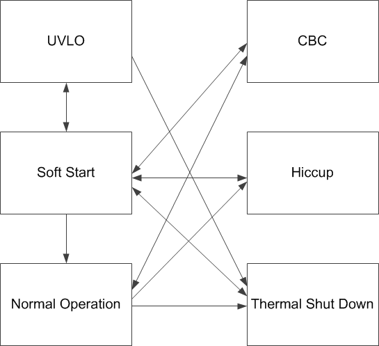
The LM5025A active clamp voltage mode PWM controller has six functional modes:
- UVLO Mode
- Soft-Start Mode
- Normal Operation Mode
- Cycle-by-Cycle Current Limit Mode
- Hiccup Mode
- Thermal Shut Down Mode
 Figure 13. Functional Mode Transition Diagram