SNVS215D April 2003 – November 2015 LM5030
PRODUCTION DATA.
- 1 Features
- 2 Applications
- 3 Description
- 4 Revision History
- 5 Pin Configuration and Functions
- 6 Specifications
- 7 Detailed Description
- 8 Application and Implementation
- 9 Power Supply Recommendations
- 10Layout
- 11Device and Documentation Support
- 12Mechanical, Packaging, and Orderable Information
Package Options
Mechanical Data (Package|Pins)
Thermal pad, mechanical data (Package|Pins)
- DPR|10
Orderable Information
8 Application and Implementation
NOTE
Information in the following applications sections is not part of the TI component specification, and TI does not warrant its accuracy or completeness. TI’s customers are responsible for determining suitability of components for their purposes. Customers should validate and test their design implementation to confirm system functionality.
8.1 Application Information
The LM5030 is a highly integrated PWM controller that contains all of the features necessary for implementing push-pull topology power converters. The device targets DC-DC converter applications with input voltages of up to 100 VDC and output power in the range 15 W to 150 W.
8.2 Typical Application
The schematic in Figure 8 shows an example of a 33-W push-pull converter controlled by a LM5030. The operating input range is 36 V to 75 V, and the output voltage is 3.3 V. The output current capability is 10 A. The converter is configured for input current protection with cycle-by-cycle current limit. An auxiliary winding is used to raise the VCC voltage to reduce the controller power dissipation.
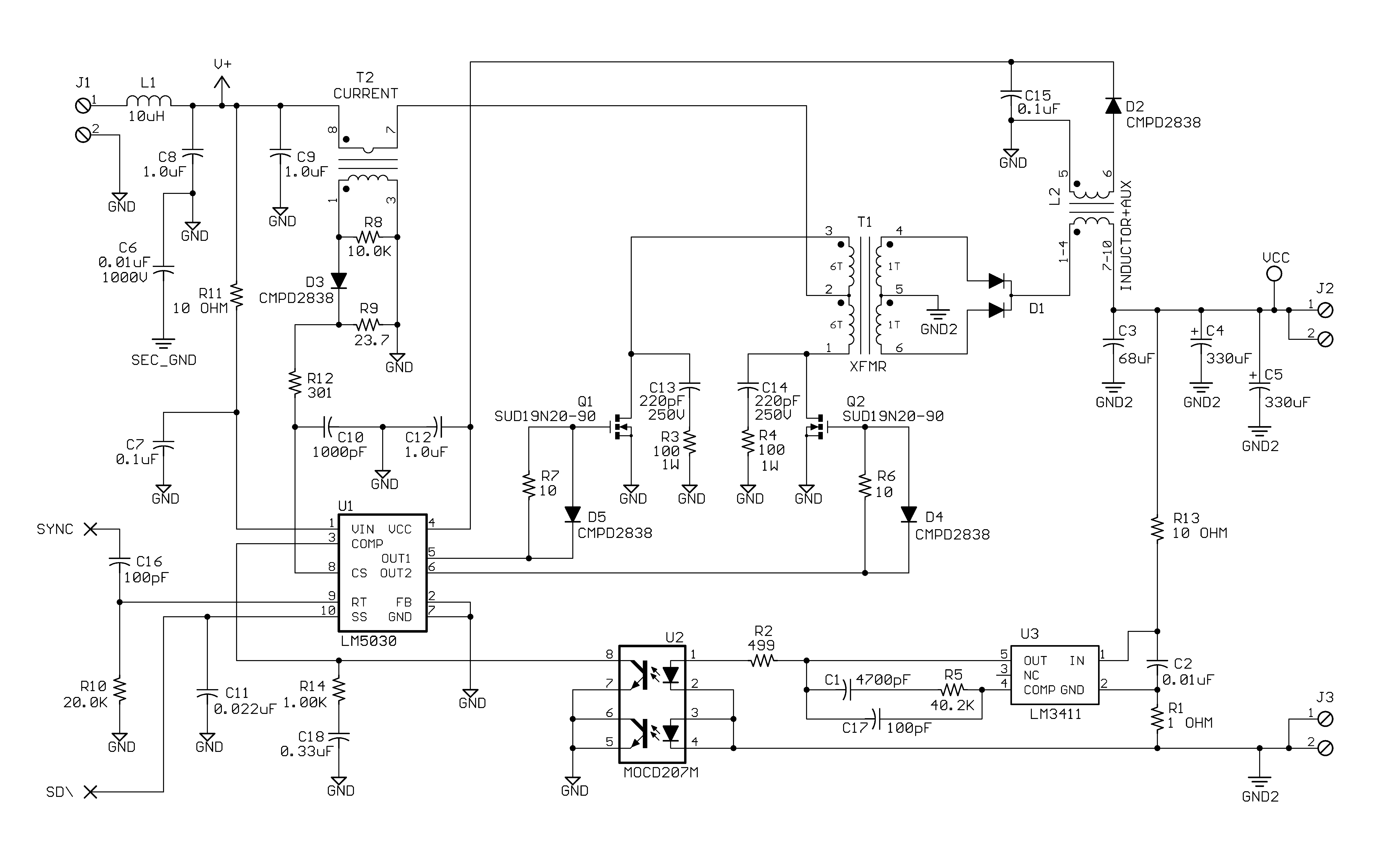 Figure 8. Typical Application Circuit, 36-V to 75-V IN and 3.3-V, 10-A OUT
8.2.1 Design Requirements
For this design example, use the input parameters listed in Table 1.
Table 1. Design Parameters
| PARAMETER | MIN | NOM | MAX | UNIT |
|---|---|---|---|---|
| Input Voltage | 36 | 75 | V | |
| Output Voltage | 3.3 | V | ||
| Output Current | 0 | 10 | A | |
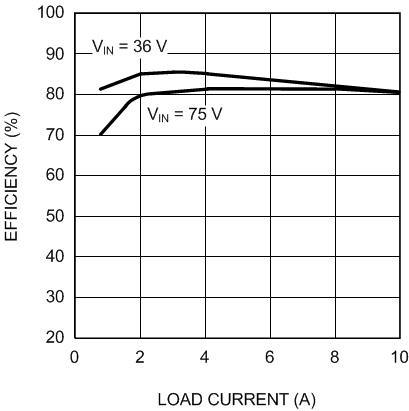
| Efficiency (Full Load) | 82.5% | |||
| Efficiency (Half Load) | 84.5% | |||
| Load Regulation | 1% | |||
| Line Regulation | 0.15% | |||
| Output Current Limit | 11 | A |
8.2.2 Detailed Design Procedure
8.2.2.1 VCC
While the LM5030 internally generates a voltage at VCC (7.7 V), the internal regulator is used mainly during the start-up sequence. Once the load current begins flowing through L2, which is both an inductor for the output filter and a transformer, a voltage is generated at the secondary of L2, which powers the VCC pin. When the externally applied voltage exceeds the internal value (7.7 V), the internal regulator shuts off, thereby reducing internal power dissipation in the LM5030. L2 is constructed such that the voltage supplied to VCC ranges from approximately 10.6 V to approximately 11.3 V, depending on the load current (see Figure 9).
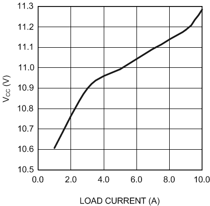 Figure 9. VCC Voltage vs Load Current
8.2.2.2 Current Sense
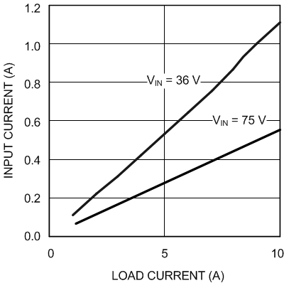
Monitoring the input current provides a good indication of the operation of the circuit. If an overload condition should exist at the output (a partial overload or a short circuit), the input current would rise above the nominal value shown in Figure 12. Transformer T2, in conjunction with D3, R9, R12 and C10, provides a voltage to pin 8 on the LM5030 (CS) which is representative of the input current flowing through its primary. The average voltage seen at pin 8 is plotted in Figure 10. If the voltage at the first current sense comparator exceeds 0.5 V, the LM5030 disables its outputs, and the circuit enters a cycle-by-cycle current limit mode. If the second level threshold (0.625 V) is exceeded due to a severe overload and transformer saturation, the LM5030 will disable its outputs and initiate a softstart sequence. However, the very short propagation delay of the cycle-by-cycle current limiter (CS1), the design of the CS filter (R9, R12, and C10), and the conservative design of the output inductor (L2), may prevent the second level current threshold from being realized on this evaluation board.
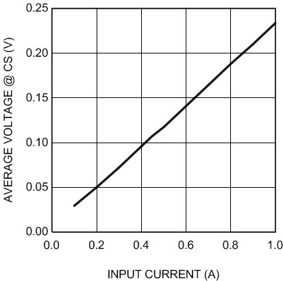 Figure 10. Average Voltage at the CS Pin vs Input Current
8.2.2.3 Shutdown
The Shutdown pad (SD) on the board connects to the SoftStart pin on the LM5030 (pin 10), and permits on/off control of the converter by an external switch. SD should be pulled below 0.45 V, with an open collector or open drain device, to shut down the LM5030 outputs and the VCC regulator. If the voltage at the SD pad is between 1.0 and 1.5 V, a partial-on condition results, which could be disruptive to the system. Therefore, the voltage at the SD pad should transition quickly between its open circuit voltage (4.9 V) and ground.
8.2.2.4 External Sync
Although the LM5030 includes an internal oscillator, its operating frequency can be synchronized to an external signal if desired. The external source frequency must be higher than the internal frequency set with the RT resistor (262 kHz with RT = 20 kΩ). The sync input pulse width must be between 15 and 150 ns, and have an amplitude of 1.5 to 3.0 V at the Sync pad on the board. The pulses are coupled to the LM5030 through a 100-pF capacitor (C16) as specified in the data sheet.
Table 2. Bill of Materials
| ITEM | PART NUMBER | DESCRIPTION | VALUE | |
|---|---|---|---|---|
| C | 1 | C0805C472K5RAC | Capacitor, CER, KEMET | 4700 p, 50 V |
| C | 2 | C0805C103K5RAC | Capacitor, CER, KEMET | 0.01 µ, 50 V |
| C | 3 | C4532X7S0G686M | Capacitor, CER, TDK | 68 µ, 4 V |
| C | 4 | T520D337M006AS4350 | Capacitor, TANT, KEMET | 330 µ, 6.3 V |
| C | 5 | T520D337M006AS4350 | Capacitor, TANT, KEMET | 330 µ, 6.3 V |
| C | 6 | C4532X7R3A103K | Capacitor, CER, TDK | 0.01 µ, 1000 V |
| C | 7 | C3216X7R2A104K | Capacitor, CER, TDK | 0.1 µ, 100 V |
| C | 8 | C4532X7R2A105M | Capacitor, CER, TDK | 1 µ, 100 V |
| C | 9 | C4532X7R2A105M | Capacitor, CER, TDK | 1 µ, 100 V |
| C | 10 | C0805C102K1RAC | Capacitor, CER, KEMET | 1000 p, 100 V |
| C | 11 | C1206C223K5RAC | Capacitor, CER, KEMET | 0.022 µ, 50 V |
| C | 12 | C3216X7R1E105M | Capacitor, CER, TDK | 1 µ, 25 V |
| C | 13 | C3216COG2J221J | Capacitor, CER, TDK | 220 p, 630 V |
| C | 14 | C3216COG2J221J | Capacitor, CER, TDK | 220 p, 630 V |
| C | 15 | C1206C104K5RAC | Capacitor, CER, KEMET | 0.1 µ, 50 V |
| C | 16 | C0805C101J1GAC | Capacitor, CER, KEMET | 100 p, 100 V |
| C | 17 | C0805C101J1GAC | Capacitor, CER, KEMET | 100 p, 100 V |
| C | 18 | C3216X7R1H334K | Capacitor, CER, TDK | 0.33 µ, 50 µ |
| D | 1 | MBRB3030CTL | Diode, Schottky, ON | |
| D | 2 | CMPD2838-NSA | Diode, Signal, Central | |
| D | 3 | CMPD2838-NSA | Diode, Signal, Central | |
| D | 4 | CMPD2838-NSA | Diode, Signal, Central | |
| D | 5 | CMPD2838-NSA | Diode, Signal, Central | |
| L | 1 | MSS6132-103 | Input Choke, Coilcraft | 10 µH, 1.5 A |
| L | 2 | A9785-B | Output Choke, Coilcraft | 7 µH |
| R | 1 | CRCW12061R00F | Resistor | 1 |
| R | 2 | CRCW12064990F | Resistor | 499 |
| R | 3 | CRCW2512101J | Resistor | 100, 1 W |
| R | 4 | CRCW2512101J | Resistor | 100, 1 W |
| R | 5 | CRCW12064022F | Resistor | 40.2K |
| R | 6 | CRCW120610R0F | Resistor | 10 |
| R | 7 | CRCW120610R0F | Resistor | 10 |
| R | 8 | CRCW12061002F | Resistor | 10K |
| R | 9 | CRCW120623R7F | Resistor | 23.7 |
| R | 10 | CRCW12062002F | Resistor | 20K |
| R | 11 | CRCW120610R0F | Resistor | 10 |
| R | 12 | CRCW12063010F | Resistor | 301 |
| R | 13 | CRCW120610R0F | Resistor | 10 |
| R | 14 | CRCW12061001F | Resistor | 1K |
| TX | 1 | A9784-B | POWER XFR, COILCRAFT | |
| TX | 2 | P8208T | CURRENT XFR, Pulse | 100:1 |
| U1 | 1 | LM5030 | REGULATOR, TI | |
| U2 | 2 | MOCD207M | OPTO-COUPLER, QT OPTOELECTRONICS | |
| U3 | 3 | LM3411AM5-3.3 | REFERENCE, TI | |
| 651-1727010 | DUAL TERMINALS, MOUSER | 3 per ASSY | ||
| X | 1 | SUD19N20-90 | FET, N, 200 V, SILICONIX | |
| X | 2 | SUD19N20-90 | FET, N, 200 V, SILICONIX | |
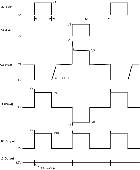 Figure 11. Representative Waveforms
Table 3. Test Data
| VIN | IOUT | t1 | t2 | Fs | V1 | V2 | V3 | V4 | V5 | V6 | V7 | V8 | V9 | V10 |
|---|---|---|---|---|---|---|---|---|---|---|---|---|---|---|
| 36 V | 1.0 A | 2.2 µS | 5.3 µS | 266.7 | 10.5 V | 36 V | 72 V | 90 V | 10 V | 6 V | –10 V | –6 V | 10 V | 6 V |
| 48 V | 10 A | 1.9 µS | 5.5 µS | 270.3 | 11.5 V | 48 V | 96 V | 130 V | 18 V | 8 V | –18 V | –8 V | 13 V | 8 V |
| 75 V | 1.0 A | 1.2 µS | 6.2 µS | 270.3 | 10.5 V | 75 V | 150 V | 200 V | 20 V | 13 V | –20 V | –13 V | 20 V | 13 V |
8.2.3 Application Curves
