SNVS344B March 2005 – December 2014 LM5032
PRODUCTION DATA.
- 1 Features
- 2 Applications
- 3 Description
- 4 Revision History
- 5 Pin Configuration and Functions
- 6 Specifications
-
7 Detailed Description
- 7.1 Overview
- 7.2 Functional Block Diagram
- 7.3
Feature Description
- 7.3.1 Line Undervoltage Lock Out, UVLO, Shutdown
- 7.3.2 Startup Regulator, VIN, VCC
- 7.3.3 Drivers Off, VCC Disable
- 7.3.4 Oscillator
- 7.3.5 PWM Comparator/Slope Compensation
- 7.3.6 Cycle-by-Cycle Current Limit
- 7.3.7 Hiccup Mode Current Limit Restart
- 7.3.8 Soft-Start
- 7.3.9 Output Duty Cycle
- 7.3.10 Driver Outputs
- 7.3.11 Thermal Shutdown
- 7.4 Device Functional Modes
-
8 Application and Implementation
- 8.1 Application Information
- 8.2 Typical Application
- 9 Power Supply Recommendations
- 10Layout
- 11Device and Documentation Support
- 12Mechanical, Packaging, and Orderable Information
Package Options
Mechanical Data (Package|Pins)
- PW|16
Thermal pad, mechanical data (Package|Pins)
Orderable Information
8 Application and Implementation
NOTE
Information in the following applications sections is not part of the TI component specification, and TI does not warrant its accuracy or completeness. TI’s customers are responsible for determining suitability of components for their purposes. Customers should validate and test their design implementation to confirm system functionality.
8.1 Application Information
8.1.1 VIN
The voltage applied to the VIN pin, normally the same as the system voltage applied to the power transformer’s primary (VPWR), can vary in the range of 13 to 100V with transient capability to 105V. The current into VIN depends primarily on the output driver capacitive loads, the switching frequency, and any external load at VCC. If the power dissipation associated with the VIN current exceeds the package capability, an external voltage should be applied to VCC (see Figure 2 & Figure 3) to reduce power in the internal start-up regulator. It is recommended the circuit of Figure 19 be used to suppress transients which may occur at the input supply, in particular where VIN is operated close to the maximum operating rating of the LM5032.
When all internal bias currents for the LM5032 and output driver currents are supplied through VIN and the internal VCC regulator, the required input current (IIN) is shown in Figure 2 & Figure 3. In most applications, upon turn-on, IIN increases with VIN as shown in Figure 2 until the UVLO threshold is reached. After the outputs are enabled and the external VCC supply voltage is active, the current into VIN then drops to a nominal 120 µA.
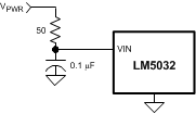 Figure 19. Input Transient Protection
8.1.2 For Applications > 100 V
For applications where the system input voltage (VPWR) exceeds 100V, VIN can be powered from an external start-up regulator as shown in Figure 20, or from any other low voltage source as shown in Figure 21. Connecting VIN and VCC together allows the LM5032 to be operated with VIN below 13V. The voltage at VCC must not exceed 15V. The voltage source at the right side of Figure 20 is typically derived from the power stage, and becomes active once the LM5032’s outputs are active.
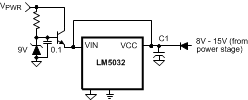 Figure 20. Start-up Regulator for VPWR >100V
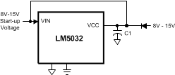 Figure 21. Bypassing the Internal Start-up Regulator
8.1.3 UVLO
The under-voltage lockout threshold (UVLO) is internally set at 1.25V at the UVLO pin. With two external resistors as shown in Figure 22, the LM5032 is enabled when VPWR exceeds the programmed threshold voltage. When VPWR is above the threshold, the internal 20 µA current source is enabled to raise the voltage at the UVLO pin, providing hysteresis. R1 and R2 are determined from the following equations:

where VHYS is the desired UVLO hysteresis at VPWR, and VPWR in the second equation is the turn-on voltage. For example, if the LM5032 is to be enabled when VPWR reaches 20V, and disabled when VPWR is decreased to 17V, R1 calculates to 150 kΩ, and R2 calculates to 10 kΩ. The voltage at UVLO should not exceed 6V at any time.
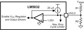 Figure 22. UVLO Circuit
The LM5032 can be remotely shutdown by taking the UVLO pin below 1.25V with an external open collector or open drain device, as shown in Figure 23. The outputs, and the VCC regulator, are disabled, and the LM5032 enters a low power mode. To shut down one regulator without affecting the other, see the Soft-start section.
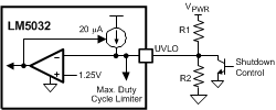 Figure 23. Shutdown Control
8.1.4 VCC
The capacitor at VCC provides not only regulator noise filtering and stability, but also prevents VCC from dropping to the lower under-voltage threshold level (UVT = 6.2V) when the output drivers source current surges to the external MOSFET gates. Additionally, the capacitor provides a necessary time delay during startup. The time delay allows the internal circuitry of the LM5032 and associated external circuitry to stabilize before VCC reaches the upper UVT threshold level (7.6V), at which time the outputs are enabled and the soft-start sequence begins. VCC is nominally regulated at 7.7V. The delay to the UVT level (Figure 1) is calculated from the following:

where C1 is the capacitor at VCC and ICC(Lim) is the VCC regulator’s current limit. If the capacitor is 0.1 µF, the nominal ICC(Lim) of 22 mA provides a delay of approximately 35 µs. The capacitor value should range between 0.1 µF and 25 µF. Experimentation with the final design may be necessary to determine the optimum value for the VCC capacitor.
The average VCC regulator current required to drive the external MOSFETs is a function of the MOSFET gate capacitance and the switching frequency (see Figure 4). To ensure VCC does not droop below the lower UVT threshold, an external supply should be diode connected to VCC to provide the required current, as shown in Figure 24. The applied VCC voltage must be between 8V and 15V. Providing the VCC voltage higher than the 7.7V regulation level with an external supply shuts off the internal regulator, reducing power dissipation within the IC. Internally there is a diode from the VCC regulator output to VIN. Typically the applied voltage is derived from an auxiliary winding on the power transformer, or on the output inductor.
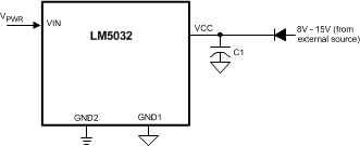 Figure 24. External Power to VCC
8.1.5 Oscillator, Sync Input
The oscillator frequency is generally selected in conjunction with the system magnetic components, and any other aspects of the system which may be affected by the frequency. The RT resistor at the RT/SYNC pin sets the frequency according to Equation 1. Each output (OUT1 and OUT2) switches at one-half the oscillator frequency. If the required frequency tolerance is critical in a particular application, the tolerance of the external resistor and the frequency tolerance specified in the Electrical Characteristics table must be considered when selecting the RT resistor.
If the LM5032 is to be synchronized to an external clock, that signal must be coupled into the RT/SYNC pin through a 100 pF capacitor. The external synchronizing frequency must be at least 4% higher than the free running frequency set by the RT resistor and no higher than twice the free running frequency. The RT/SYNC pin voltage is nominally regulated at 2.0V and the external pulse amplitude should lift the pin to between 3.8V and 5.0V on the low-to-high transition. The synchronization pulse width should be between 15 and 150 ns. The RT resistor is always required, whether the oscillator is free running or externally synchronized.
8.1.6 Voltage Feedback, COMP1, COMP2
Each COMP pin is designed to accept a voltage feedback signal from the respective regulated output via an error amplifier and (typically) an opto-coupler. A typical configuration is shown in Figure 15. VOUT is compared to a reference by the error amplifier which has an appropriate frequency compensation network. The amplifier’s output drives the opto-coupler, which in turn drives the COMP pin.
When the LM5032’s two controller channels are configured to provide a single high current output, COMP1 and COMP2 are typically connected together, and to the feedback signal from the optocoupler.
8.1.7 Current Sense, CS1, CS2
Each CS pin receives an input signal representative of its transformer’s primary current, either from a current sense transformer or from a resistor in series with the source of the primary switch, as shown in Figure 25 and Figure 26. In both cases the sensed current creates a ramping voltage across R1, and the RF/CF filter suppresses noise and transients. R1, RF and CF should be as physically close to the LM5032 as possible, and the ground connection from the current sense transformer, or R1, should be a dedicated track to the appropriate GND pin. The current sense components must provide >0.5V at the CS pin when an over-current condition exists.
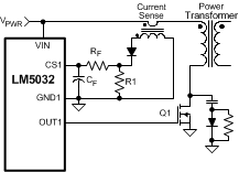 Figure 25. Current Sense Using a Current Sense Transformer
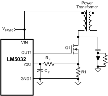 Figure 26. Current Sense Using a Source Sense Resistor (R1)
8.1.8 Hiccup Mode Current Limit Restart
This circuit’s operation is described in the Functional Description. Also see Figure 16 and Figure 17. In the case of continuous current limit detection at both CS pins, the time required to reach the 2.55V RES pin threshold is:
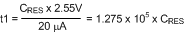
For example, if CRES = 0.1 µF the time t1 in Figure 18 is approximately 12.75 ms.
In the case of continuous current limit detection at one CS pin only, the time to reach the 2.55V threshold is increased by a factor of four, or:
The time t2 in Figure 17 is set by the capacitor at each SS pin and the internal 1 µA current source, and is equal to:
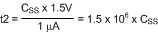
If CSS = 0.1 µF t2 is ≊150 ms. Time t3 is set by the internal 50 µA current source, and is equal to:
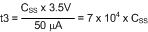
The time t2 provides a periodic dwell time for the converter in the event of a sustained overload or short circuit. This results in lower average input current and lower power dissipated within the circuit components. It is recommended that the ratio of t2/(t1 + t3) be in the range of 5 to 10 to make good use of this feature.
If the application requires no delay from the first detection of a current limit condition, so that t1 is effectively zero, the RES pin can be left open (no external capacitor). If it is desired to disable the hiccup mode current limit operation then the RES pin should be connected to ground.
8.1.9 Soft-Start
The capacitors at SS1 and SS2 determine the time required for each regulator’s output duty cycle to increase from zero to its final value for regulation. The minimum acceptable time is dependent on the output capacitance and the response of each feedback loop to the COMP pin. If the Soft-start time is too quick, the output could significantly overshoot its intended voltage before the feedback loop has a chance to regulate the PWM controller.
After power is applied and VCC has passed its upper UVT threshold (≊7.6V), the voltage at each SS pin ramps up as its external capacitor is charged up by an internal 50 µA current source (see Figure 1). The voltage at the COMP pins follow the SS pins. When both have reached ≊1.5V, PWM pulses appear at the driver outputs with very low duty cycle. The voltage at each SS pin continues to increase to ≊5.0V. The voltage at each COMP pin, and the PWM duty cycle, increase to the value required for regulation as determined by its feedback loop. The time t1 in Figure 1 is calculated from:
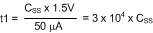
With a 0.1 µF capacitor at SS, t1 is ≊3 ms.
If the Hiccup Mode Current Limit Restart circuit activates due to repeated current limit detections at CS1 and/or CS2, both SS1 and SS2 are internally grounded (see the section on Hiccup Mode Current Limit Restart). After a short propagation delay, the SS pins are released and the external SS pin capacitors are charged by internal 1 µA current sources. The slow charge rate provides a rest or dwell time for the converter power stage (t2 in Figure 17), reducing the average input current and component temperature rise while in an overload condition. When the voltage at the SS and COMP pins reach ≊1.5V, the first pulse out of either PWM comparator switches the internal SS pin current sources to 50 µA. The voltages at the SS and COMP pins then increase more quickly, increasing the duty cycle at the output drivers. The rest time t2 is the time required for SS to reach 1.5V:
With a 0.1 µF capacitor at SS, t2 is ≊150 ms.
Experimentation with the startup sequence and over-current restart condition is usually necessary to determine the appropriate value for the SS capacitors.
To shutdown one regulator without affecting the other, ground the appropriate SS pin with an open collector or open drain device as shown in Figure 27. The SS pin forces the COMP pin to ground which reduces the PWM duty cycle to zero for that regulator. Releasing the SS pin allows normal operation to resume.
When the LM5032’s two controller channels are configured to provide a single high current output, SS1 and SS2 are typically connected together, requiring a single capacitor for the two pins.
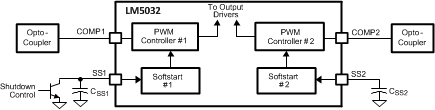 Figure 27. Shutting Down One Regulator Channel
8.1.10 Line Voltage Dependent Maximum Duty Cycle
As VPWR increases and the voltage at UVLO follows, the maximum allowed duty cycle decreases according to the graph of Figure 9. Using values from the example above (R1 = 150 kΩ, R2 = 10 kΩ in Figure 22), the maximum duty cycle varies as shown in Figure 10. If it is desired to increase the slope of the ramp in Figure 10, Figure 28 shows a suggested configuration. After the LM5032 is enabled, Z1 clamps the voltage across R1B, and UVLO increases with VPWR at a rate determined by the ratio R2/(R1A + R2).
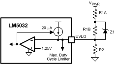 Figure 28. Altering the Slope of Duty Cycle vs. VPWR
8.1.11 User Defined Max Duty Cycle
The maximum allowed duty cycle at OUT1 and OUT2 can be set with a resistor from DCL to GND1. See Figure 8 and Equation 2. The default maximum duty cycle (80%) determined by the internal clock signals can be selected by setting RDCL = RT. The oscillator frequency setting resistor (RT) must be determined before RDCL is selected. The DCL pin should not be left open.
8.2 Typical Application
Figure 29 shows an example of an LM5032-controlled 200-W interleaved regulator which provides a single regulated 48-V output. The interleaving of two power stages to a single output reduces the ripple voltage across both input and output capacitors, and improves the power stage efficiency compared to a single-stage design. Since the two interleaved control blocks are used to regulate a single combined output, the two soft-start pins SS1 and SS2 are connected to a single soft-start capacitor, and the two COMP1 and COMP2 pins are connected together to a single error amplifier.
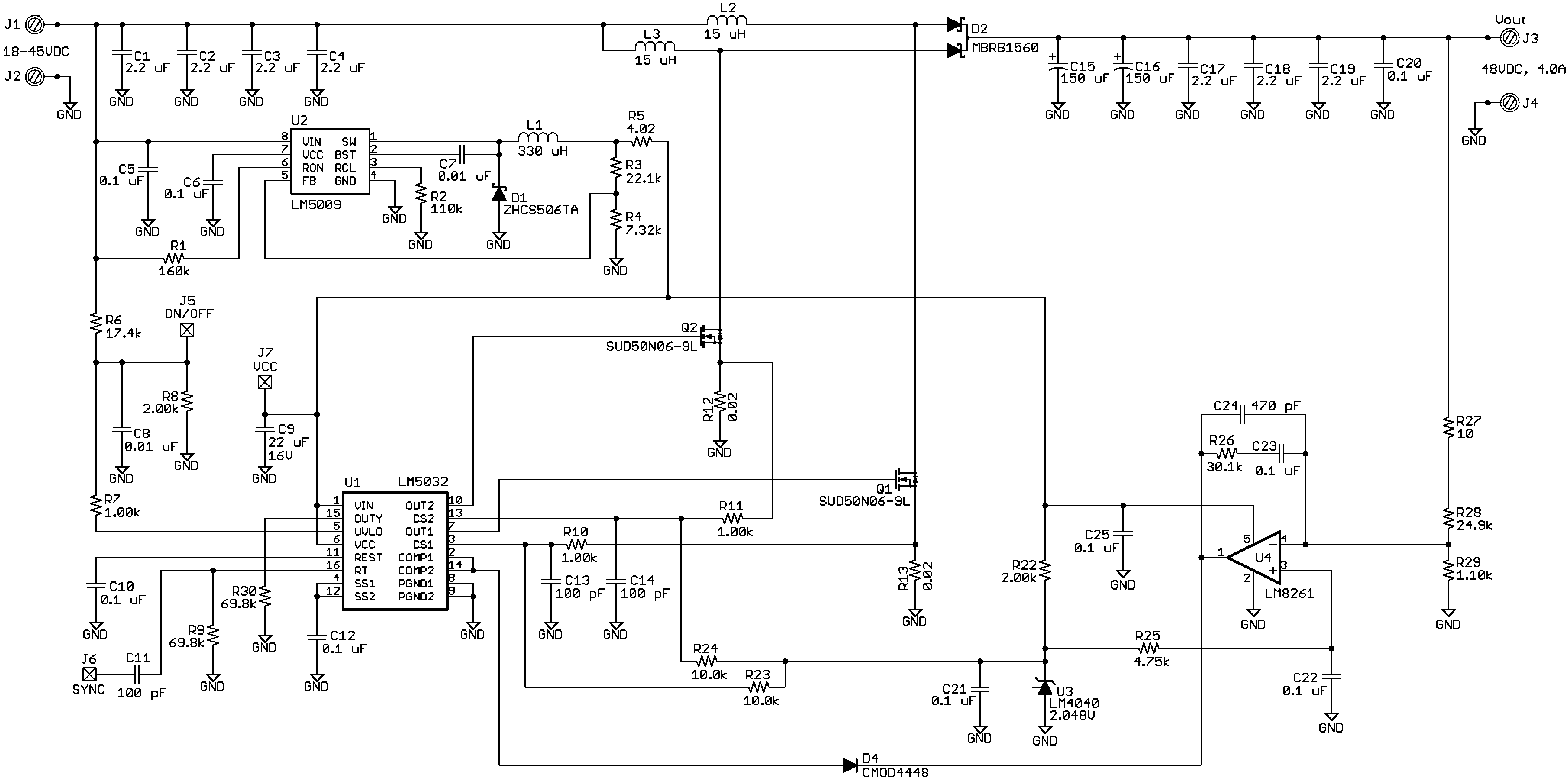 Figure 29. Evaluation Module Schematic
8.2.1 Design Requirements
| DESIGN PARAMETERS | VALUE |
|---|---|
| Input voltage range, VIN | 18 V to 45 V |
| Output voltage, VOUT | 48 V |
| Output current, IOUT | 4 A |
| Output ripple voltage, VRIPPLE(OUT) | < 2% (960 mVpp) |
| Switching frequency, FSW (per phase) | 123 kHz |
8.2.2 Detailed Design Procedure
8.2.2.1 Oscillator Frequency and Maximum Duty Cycle
The LM5032 oscillator frequency should be set at twice the target switching frequency of each interleaved power stage, for example, Fosc = 2 x Fsw.
From Equation 1, the required value of resistor on the RT pin (R9 in Figure 29) is calculated as follows:

The nearest E96 value of 69.8 kΩ is used.
The maximum duty cycle is set to 80% (see the Output Duty Cycle section) by choosing the same value resistor on the DCL pin, so R30 is also set to 69.8 kΩ.
8.2.2.2 Power Stage Design
8.2.2.2.1 Boost Inductor Selection
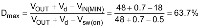
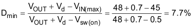
Maximum and minimum operating duty cycles are calculated at maximum and minimum input voltage, where Vd is the boost diode forward voltage drop, and Vsw(on) is the voltage drop across the boost MOSFET plus current sense element:
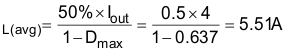
The highest average inductor current in each phase is calculated at highest load and minimum input voltage, where each phase is assumed to carry 50% of the total load current:
Allowing the peak-to-peak inductor current ripple to be 100% of the average:
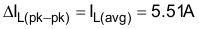
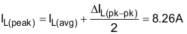
And the peak inductor current IL(peak) will be:
Knowing the switching frequency, maximum duty cycle and target peak-peak ripple current, the required inductance can be calculated:
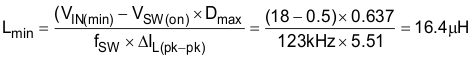
Off-the-shelf available inductors of 15 µH were used, resulting in slightly higher peak-peak inductor ripple current, and slightly higher inductor peak current.
8.2.2.2.2 Output Capacitor Selection
The output ripple across the boost output capacitor can be approximated from the following equation, where COUT is the value of output capacitance, and ESR is the equivalent-series-resistance of the output capacitance. For this design, the chosen electrolytic output capacitors are 150 μF with 160-mΩ ESR, so the net capacitance is 300 μF and net ESR is 80 mΩ.

This meets the target 2% specification. However, the extra ceramic output capacitors will also absorb a significant percentage of the switching frequency ripple, so the resulting output peak-to-peak ripple voltage should be lower than the value calculated above, and should be comfortably less than the 2% specification.
8.2.2.2.3 Boost MOSFET Selection
The boost MOSFET should be rated for at least the rated output voltage plus some margin for voltage ringing. A 60-V device was selected. Since the boost inductor value was chosen to achieve peak-to-peak ripple current equal to 100% of the average current, the RMS MOSFET current at maximum load and minimum Vin is:

The chosen 60-V rated MOSFET SUD50N06-9L has 9.3-mΩ Rds(on), resulting in approximately 200-mW conduction loss.
8.2.2.2.4 Boost Diode Selection
The boost diode must have a reverse voltage rating of at least VOUT, plus some margin for ringing. Thus a 60-V rated part was selected. Since fast reverse recovery is important, a Schottky device can be used at this voltage rating. A common-cathode dual-diode MBR1560 was selected, with each diode connected to one or other of the interleaved phases.
8.2.2.3 UVLO Setting
To ensure start-up below the required minimum system input voltage of 18 V, the UVLO divider resistors R6 and R8 are set to 17.4 kΩ and 2 kΩ, respectively. This sets the input UVLO turn-on level to:
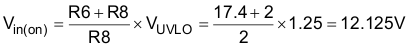
This gives plenty margin to the required 16-V minimum. Resistor R7 in series with the UVLO pin increases the effective UVLO hysteresis.
8.2.2.4 VIN, VCC, Startup
To reduce the power dissipation in the internal startup regulator on the VIN pin, a separate external switching regulator is used. This consists of U2 (LM5009) plus associated circuitry C5, C6, R1, R2, C7, D1, L1, R3 and R4. This buck regulator is designed to generate a 10-V regulated supply voltage for the VCC of U1 LM5032. See the LM5009 device datasheet, SNVS402, for detailed design information.
Since the LM5032 internal VIN regulator is not used in this design, the LM5032 VIN and VCC pins are shorted together.
8.2.2.5 Soft-Start and Overload
Since the two soft-start pins SS1 and SS2 are connected to a single soft-start capacitor, C12, the combined charging current of both soft-start pins charges the single soft-start capacitor. The soft-start delay to commencement of first PWM switching can be calculated from:

Thereafter, the soft-start ramp time will depend on the power stage design and the operating conditions (input voltage and output load).
8.2.2.6 Current Sense
In order to improve the efficiency, a lower value current sense shunt resistance is used. To enable this lower value, the normal operating range of the CS1/CS2 pins is reduced by adding an external DC offset to the CS1/CS2 pins, as shown in Figure 30.
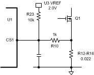 Figure 30. Current Sense DC Offset Circuit
This circuit uses the 2.048-V reference U3 to add a typical offset of 185 mV to both current-sense pins. This reduces the active range of the internal cycle-by-cycle current-limit comparator to 315 mV, allowing the current-sense shunt to be decreased to 66% of the value that would be otherwise required.
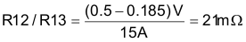
From the power stage design calculations, the peak inductor current in each power stage was approximately 9 A at max load and minimum Vin. Allowing for tolerances, and providing some margin for output overload, the current-sense shunt resistors are chosen for a peak current limit of approximately 15 A:
A standard value of 20 mΩ was used.
8.2.3 Application Curves
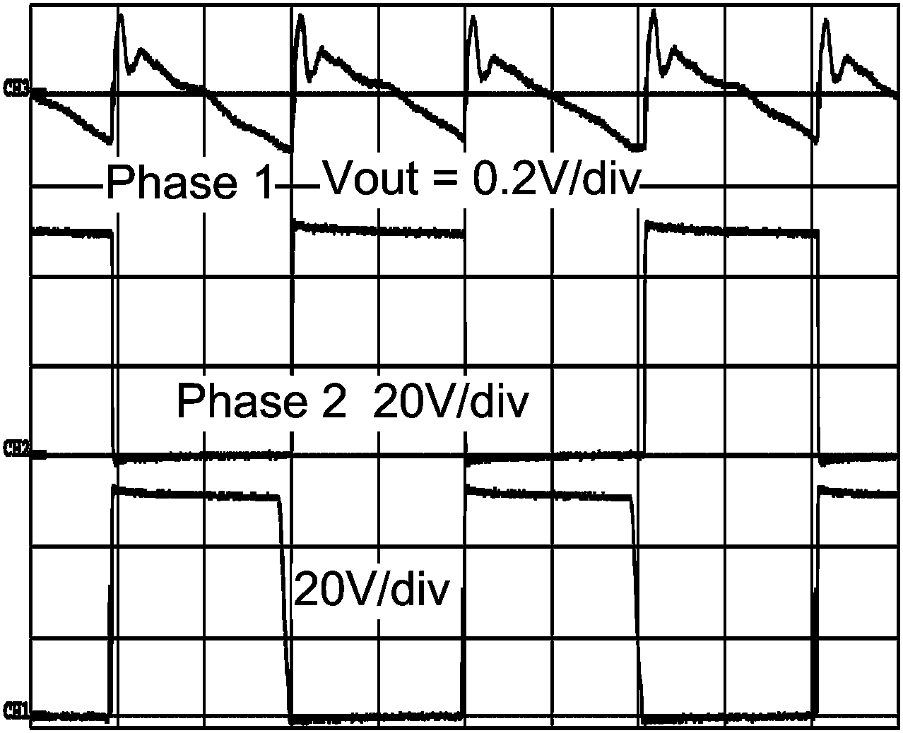
Figure 31 shows the measured efficiency as a function of load current and input voltage.
Figure 32 illustrates the switching nodes of the two interleaved phases, and the resulting output ripple at twice the switching frequency. This was measured at Vin of 24 V, where duty cycle is approx. 50% and maximum ripple-cancellation occurs.
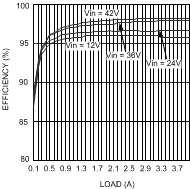
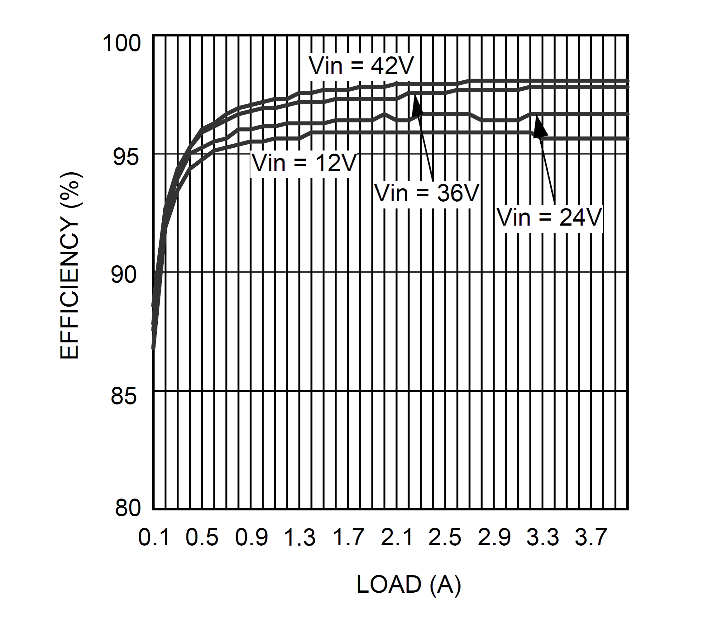 Figure 31. Efficiency vs. Load and Vin