SNVS344B March 2005 – December 2014 LM5032
PRODUCTION DATA.
- 1 Features
- 2 Applications
- 3 Description
- 4 Revision History
- 5 Pin Configuration and Functions
- 6 Specifications
-
7 Detailed Description
- 7.1 Overview
- 7.2 Functional Block Diagram
- 7.3
Feature Description
- 7.3.1 Line Undervoltage Lock Out, UVLO, Shutdown
- 7.3.2 Startup Regulator, VIN, VCC
- 7.3.3 Drivers Off, VCC Disable
- 7.3.4 Oscillator
- 7.3.5 PWM Comparator/Slope Compensation
- 7.3.6 Cycle-by-Cycle Current Limit
- 7.3.7 Hiccup Mode Current Limit Restart
- 7.3.8 Soft-Start
- 7.3.9 Output Duty Cycle
- 7.3.10 Driver Outputs
- 7.3.11 Thermal Shutdown
- 7.4 Device Functional Modes
-
8 Application and Implementation
- 8.1 Application Information
- 8.2 Typical Application
- 9 Power Supply Recommendations
- 10Layout
- 11Device and Documentation Support
- 12Mechanical, Packaging, and Orderable Information
Package Options
Mechanical Data (Package|Pins)
- PW|16
Thermal pad, mechanical data (Package|Pins)
Orderable Information
10 Layout
10.1 Layout Guidelines
The LM5032 Current Sense and PWM comparators are very fast, and respond to short duration noise pulses. The components at the CS, COMP, SS, DCL, UVLO, and the RT/SYNC pins should be as physically close as possible to the IC, thereby minimizing noise pickup in the PC board tracks.
Layout considerations are critical for the current sense filter. If current sense transformers are used, both leads of each transformer secondary should be routed to the sense filter components and to the IC pins. The ground side of each transformer should be connected via a dedicated PC board track to its appropriate GND pin, rather than through the ground plane.
If the current sense circuits employ sense resistors in the drive transistor sources, low inductance resistors should be used. In this case, all the noise sensitive low current ground tracks should be connected in common near the IC, and then a single connection made to the power ground (sense resistor ground point). The outputs of the LM5032 should have short direct paths to the power MOSFETs in order to minimize inductance in the PC board traces.
The two ground pins (GND1, GND2) must be connected together with a short direct connection to avoid jitter due to relative ground bounce in the operation of the two regulators.
If the internal dissipation of the LM5032 produces high junction temperatures during normal operation, the use of wide PC board traces can help conduct heat away from the IC. Judicious positioning of the PC board within the end product, along with use of any available air flow (forced or natural convection) can help reduce the junction temperatures.
10.2 Layout Example
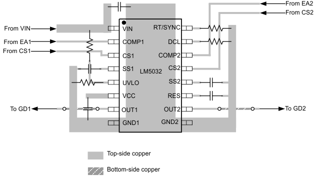 Figure 33. Layout Example