SNVS344B March 2005 – December 2014 LM5032
PRODUCTION DATA.
- 1 Features
- 2 Applications
- 3 Description
- 4 Revision History
- 5 Pin Configuration and Functions
- 6 Specifications
-
7 Detailed Description
- 7.1 Overview
- 7.2 Functional Block Diagram
- 7.3
Feature Description
- 7.3.1 Line Undervoltage Lock Out, UVLO, Shutdown
- 7.3.2 Startup Regulator, VIN, VCC
- 7.3.3 Drivers Off, VCC Disable
- 7.3.4 Oscillator
- 7.3.5 PWM Comparator/Slope Compensation
- 7.3.6 Cycle-by-Cycle Current Limit
- 7.3.7 Hiccup Mode Current Limit Restart
- 7.3.8 Soft-Start
- 7.3.9 Output Duty Cycle
- 7.3.10 Driver Outputs
- 7.3.11 Thermal Shutdown
- 7.4 Device Functional Modes
-
8 Application and Implementation
- 8.1 Application Information
- 8.2 Typical Application
- 9 Power Supply Recommendations
- 10Layout
- 11Device and Documentation Support
- 12Mechanical, Packaging, and Orderable Information
Package Options
Mechanical Data (Package|Pins)
- PW|16
Thermal pad, mechanical data (Package|Pins)
Orderable Information
7 Detailed Description
7.1 Overview
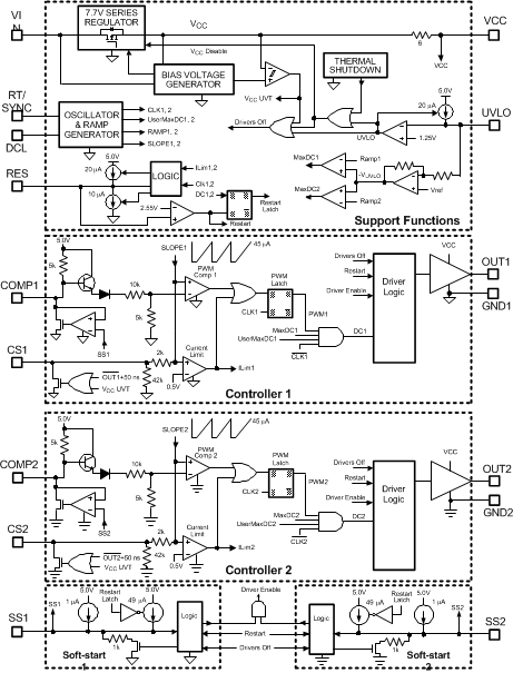
The LM5032 contains all the features necessary to implement two independently regulated current mode dc/dc converters, or a single high current converter comprised of two parallel interleaved channels using the Forward converter topology. The two controllers operate 180° out of phase from a common oscillator, thereby reducing input ripple current. Each regulator channel contains a complete PWM controller, current sense input, soft-start circuit, and gate driver output. Common to both channels are the startup and VCC regulator, line under-voltage lockout, 2 MHz capable oscillator, maximum duty cycle control, and the hiccup mode fault protection circuit.
The gate driver outputs (OUT1, OUT2) are designed to drive N-channel MOSFETs. Their compound configuration reduces the turn-off-time, thereby reducing switching losses. Additional features include thermal shutdown, slope compensation, and the oscillator synchronization capability.
7.2 Functional Block Diagram
7.3 Feature Description
7.3.1 Line Undervoltage Lock Out, UVLO, Shutdown
The LM5032 contains a line under-voltage lockout circuit (UVLO) designed to enable the VCC regulator and output drivers when the system voltage (VPWR) exceeds the desired level (see Figure 14). VPWR is the voltage normally applied to the transformer primary, and usually connected to the VIN pin (see the schematic on Page 1). The threshold at the UVLO comparator is 1.25V. An external resistor divider connected from VPWR to ground provides 1.25V at the UVLO pin when VPWR is increased to the desired turn-on threshold. When VPWR is below the threshold the VCC regulator and output drivers are disabled, and the internal 20 µA current source is off. When VPWR reaches the threshold, the comparator output switches low to enable the internal circuits and the 20 µA current source. The 20 µA flows into the external divider’s junction, raising the voltage at UVLO, thereby providing hysteresis. Internally the voltage at UVLO also drives the Maximum Duty Cycle Limiter circuit (described below), which may influence the values chosen for the UVLO pin resistors. At maximum VPWR, the voltage at UVLO should not exceed 6V. Refer to the Applications Information section for a procedure to calculate the resistors values.
The LM5032 controller can be shutdown by forcing the UVLO pin below 1.25V with an external switch. When the UVLO pin is low, the outputs and the VCC regulator are disabled, and the LM5032 enters a low power mode. If VCC pin is not powered from an external source, the current into VIN drops to a nominal 500 µA. If the VCC pin is powered from an external source, the current into VIN is nominally 50 µA, and the current into the VCC pin is approximately 4.3 mA. To disable one regulator without affecting the other, see the description of the Soft-start section.
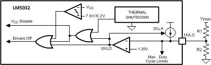 Figure 14. Drivers Off and VCC Disable
7.3.2 Startup Regulator, VIN, VCC
The high voltage startup regulator is integral to the LM5032. The input pin VIN can be connected directly to a voltage between 13V and 100V, with transient capability to 105V. The startup regulator provides bias voltages to the series pass VCC regulator and the UVLO circuit. The VCC regulator is disabled until the voltage at the UVLO pin (described above) exceeds 1.25V. For applications where VPWR exceeds 100V the internal startup regulator can be powered from an external startup regulator or other available low voltage source. See the Applications Information section for details.
The VCC under-voltage threshold circuit (UVT) monitors the VCC regulator output. When the series pass regulator is enabled and the internal VCC voltage increases to > 7.6V, the UVT comparator activates the PWM controller and output drivers via the Drivers Off signal. The UVT comparator has built-in hysteresis, with the lower threshold nominally set to 6.2V. See Figure 1 and Figure 14.
When enabled, the VCC regulated output is 7.7V ±4% with current limited to a minimum of 19 mA (typically 22 mA). The regulator’s output impedance is ≊ 6Ω.
The VCC pin requires a capacitor to ground for stability, as well as to provide the surge currents to the external MOSFETs via the gate driver outputs. The capacitor should be physically close to the VCC and GND pins.
In most applications it is necessary to power VCC from an external source as the average current required at the output drivers may exceed the current capability of the internal regulator and/or the thermal capability of the LM5032 package (see Figure 4). Normally the external source is derived from the converter’s power stage once the LM5032 outputs are active. Refer to the Applications Information section for more information.
7.3.3 Drivers Off, VCC Disable
Referring to Figure 14, Drivers Off and VCC Disable are internal signals which, when active disable portions of the LM5032. If the UVLO pin is below 1.25V, or if the thermal shutdown activates, the VCC Disable line switches high to disable the VCC regulator. UVLO also activates the Drivers Off signal to disable the output drivers, connect the SS1, SS2, COMP1, COMP2 and RES pins to ground, and enable the 50 µA Soft-start current sources.
If the VCC voltage falls below the under-voltage threshold of 6.2V , the UVT comparator activates only the Drivers Off signal. The output drivers are disabled but the VCC regulator is not disabled. Additionally, the CS1, CS2, SS1, SS2, COMP1, COMP2 and RES pins are internally grounded, and the 50 µA Soft-start current sources are enabled.
7.3.4 Oscillator
The oscillator frequency is set with an external resistor RT connected between the RT/SYNC and GND1 pins. The resistor value is calculated from:
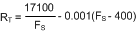
where FS is the desired oscillator frequency in kHz (maximum of 2 MHz), and RT is in kΩ. See Figure 7. The two gate driver outputs (OUT1 and OUT2) switch at half the oscillator frequency and 180° out of phase with each other. The voltage at the RT/SYNC pin is internally regulated at 2.0V. The RT resistor should be located as close as possible to the LM5032 with short direct connections to the pins.
The LM5032 can be synchronized to an external clock by applying a narrow clock pulse to the RT/SYNC pin. See the Applications Information section for details on this procedure. The RT resistor is always required, whether the oscillator is free running or externally synchronized.
7.3.5 PWM Comparator/Slope Compensation
The PWM comparator of each controller compares a slope compensated current ramp signal with the loop error voltage derived from the COMP pin. The COMP voltage is typically controlled by an external error amplifier/optocoupler feedback circuit to regulate the converter output voltage. Internally, the voltage at the COMP pin passes through two level shifting diodes and a gain reducing 3:1 resistor divider (see Figure 15). The compensated current ramp signal is a combination of the current waveform at the CS pin, and an internally generated ramp derived from the internal clock. At duty cycles greater than 50% current mode control circuits are prone to subharmonic oscillation. By adding a small fixed ramp to the external current sense signal oscillations can be avoided. The internal ramp has an amplitude of 45 µA and is sourced into an internal 2kΩ resistor, and a 42 kΩ resistor in parallel with the external impedance at the CS pin. The ramp current also flows through the external impedance connected to the CS pin and thus, the amount of slope compensation can be adjusted by varying the external circuit at the CS pin.
The output of the PWM comparator provides the pulse width information to the output drivers. This comparator is optimized for speed in order to achieve minimum controllable duty cycles. The comparator’s output duty cycle is 0% for VCOMP ≤1.5V, and increases as VCOMP increases.
If either Soft-start pin is pulled low (internally or externally) the corresponding COMP pin is pulled down with it, forcing the output duty cycle to zero. When the Soft-start pin voltage increases, the COMP pin is allowed to increase. An internal 5 kΩ resistor connected from COMP to an internal 5.0V supply provides a pull-up for the COMP pin and bias current to the collector of the opto-coupler transistor.
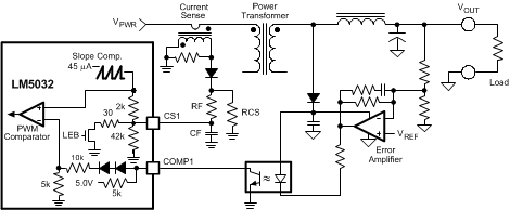 Figure 15. Typical Feedback Network
7.3.6 Cycle-by-Cycle Current Limit
Each CS pin is designed to accept a signal representative of its transformer primary current. If the voltage at CS exceeds 0.5V the current sense comparator terminates the present main output driver (OUT pin) pulse. If the high current fault persists, the controller operates with constant peak switch current in a cycle-by-cycle current limit mode, and a Hiccup Mode Current Limit Restart cycle begins (see below).
Each CS pin is internally connect to ground through a 30Ω resistor during the main output off time to discharge external filter capacitance. The discharge device remains on for an additional 50 ns after the main output driver switches high to blank leading edge transients in the current sensing circuit. Discharging the CS pin filter each cycle and blanking leading edge spikes reduces the filter requirement which improves the current sense response time.
The current sense comparators are fast and respond to short duration noise pulses. The external circuitry at each CS pin should include an R-C filter to suppress noise. Layout considerations are critical for the current sense filter and the sense resistor. Refer to the Applications Information section for PC board layout guidelines.
7.3.7 Hiccup Mode Current Limit Restart
If cycle-by-cycle current limiting continues in either or both controllers for a sufficient period of time, the Current Limit Restart circuit disables both regulators and initiates a soft-start sequence after a programmable delay. The duration of cycle-by-cycle current limiting before turn-off occurs is programmed by the value of the external capacitor at the RES pin. The dwell time before output switching resumes is programmed by the value of the Soft-start capacitor(s). The circuit is detailed in Figure 16 and the timing is shown in Figure 17. A description of this circuit’s operation is as follows:
a) No current limit detected:
The 10 µA discharge current source at RES is enabled pulling the RES pin to ground.
b) Current limit repeatedly detected at both CS inputs:
The 20 µA current source at RES is enabled continuously to charge the RES pin capacitor as shown in Figure 17. The current limit comparators also terminate the PWM output pulses to provide a cycle-by-cycle current limiting. When the voltage on the RES capacitor reaches the 2.55V restart comparator threshold, the comparator sets the Restart Latch which produces the following restart sequence:
- The SS1 and SS2 pin charging currents are reduced from 50µA to 1 µA.
- An internal MOSFET is turned on to discharge the RES pin capacitor.
- The internal MOSFETs at SS1 and SS2 are turned on to discharge the Soft-start capacitors.
- COMP1 and COMP2 follow SS1 and SS2 respectively and reduce the PWM duty cycles to zero.
- When the voltages at the SS pins fall below 200mV, the internal MOSFETs at the SS pins are turned off allowing the SS pins to be charged by the 1µA current sources.
- When either SS pin reaches ≊1.5V its PWM controller produces the first pulse of a soft-start sequence which resets the Restart Latch. The SS charging currents are increased to 50 µA and the soft-start sequence continues at the normal rate.
If the overload condition still exists, the voltage at RES begins to increase again and repeat the restart cycle as shown in Figure 17. If the overload condition has been cleared, the RES pin is held at ground by the 10 µA current source.
c) Current limit repeatedly detected at one of the two CS inputs:
In this condition the RES pin capacitor is charged by the 20 µA current source once each clock cycle of the current limited regulator, and discharged by the 10 µA current source once each clock cycle of the unaffected regulator. The voltage at the RES pin increases one fourth as fast as in case b) described above. The current limited regulator operates in a cycle-by-cycle current limit mode until the voltage at RES reaches the 2.55V threshold. When the Restart Comparator output switches high the Restart Latch is set, both SS pin capacitors are discharged to disable the regulator channels, and a restart sequence begins as described in case b) above.
To determine the value of the RES pin capacitor, see the Applications Information section.
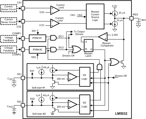 Figure 16. Current Limit Restart Circuit
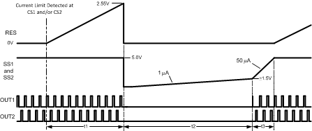 Figure 17. Current Limit Restart Timing
7.3.8 Soft-Start
Each soft-start circuit allows the corresponding regulator to gradually reach a steady state operating point, thereby reducing startup current surges and output overshoot. Upon turn-on, both SS pins are internally held at ground. When VCC increases past its under-voltage threshold (UVT), the SS pins are released and internal 50 µA current sources charge the external capacitors. The voltage at each COMP pin follows the SS pin, and when COMP reaches ≊1.5V, the output pulses commence at a low duty cycle. The voltage at the SS pins continues to increase and saturates at ≊5.0V, The voltage at each COMP pin increases to the value required for regulation where it is controlled by its voltage feedback loop (see Figure 1).
If the internal Drivers Off line is activated (see Drivers Off, VCC Disable), both SS pins are internally grounded. The SS pins pull the COMP pins to ground while the Driver Off signal disables the output drivers. When the event which activated the Drivers Off line is cleared and Vcc exceeds its under-voltage threshold, the SS pins are released. The internal 50 µA current sources then charge the external soft-start capacitors allowing each regulator’s output duty cycle to increase.
If the Current Limit Restart threshold is reached due to repeated over-current detections, both SS pins (and the COMP pins) are pulled to ground. The output drivers are disabled, and the 50 µA SS pin current sources are reduced to 1 µA. After a short propagation delay the SS pins and the COMP pins are released, and the external capacitors are charged up at a slow rate. When the COMP voltage reaches ≊ 1.5V, the output drivers are enabled, and the current sources at the SS pins are increased to 50 µA. The output duty cycle then increases to the value required for regulation.
To shutdown one regulator without affecting the other, ground the appropriate SS pin. This forces the COMP pin to ground, reducing the output duty cycle to zero for that regulator. Releasing the SS pin allows normal operation to resume.
7.3.9 Output Duty Cycle
The output driver’s duty cycle for each controller is normally controlled by comparing the voltage provided to the COMP input by the external voltage feedback circuit with the current information at the CS pin. However, the maximum duty cycle during transient or fault conditions may be intentionally limited by two other circuits, both of which are common to the two controller channels.
User Defined Maximum Duty Cycle. The maximum allowed duty cycle can be set with the RDCL resistor connected from the DCL pin to GND1, according to the following equation:
RT is the oscillator frequency programming resistor connected to the RT/SYNC pin. The value of the RDCL resistor must be calculated after the RT resistor is selected. See Figure 8. Referring to the block diagram of the voltage at the DCL pin is compared to the Ramp1 and Ramp2 signals, creating the UserMaxDC1 and UserMaxDC2 timing signals. These signal are provided to the two 4-input AND gates to limit the PWM duty cycle of both channels.
Line Voltage Maximum Duty Cycle. The voltage at the UVLO pin, normally proportional to the voltage at VPWR, further limits the maximum duty cycle at high input voltages. Referring to Figure 10, when the UVLO pin is below 1.25V, the outputs are disabled. At UVLO = 1.25V the maximum allowed duty cycle is 80% (or less if limited by the DCL resistor). As the UVLO pin voltage increases with VPWR, the maximum duty cycle decreases, reaching a minimum of 10% at ≊4.5V. Referring to the UVLO voltage, after passing through an inverting gain stage, is compared to the Ramp1 and Ramp2 signals generated by the oscillator. The output of these comparators are the MaxDC1 and MaxDC2 timing signals. These signals are provided to the two 4-input AND gates which limit the PWM pulses delivered to the output drivers.
Resulting Output Duty Cycle. The controller duty cycle is determined by the four signals into the 4-input AND gates in (UserMaxDC, MaxDC, PWM and CLK). The output driver pulsewidth is equal to the least of these four pulses. Whichever input of the AND gate transitions high-to-low first terminates the output driver’s on-time.
7.3.10 Driver Outputs
OUT1, the primary switch driver for Controller 1 is designed to drive the gate of an N-channel MOSFET with 1.5A sourcing current and 2.5A sinking current. The peak output levels are VCC and GND1. The ground return path for Controller 1 is GND1. The corresponding pins for Controller 2 are OUT2 and GND2.
OUT1 and OUT2 are compound gate drivers with CMOS and Bipolar output transistors as shown in Figure 18. The parallel MOS and Bipolar devices provide a faster turn-off of the primary switch thereby reducing switching losses. The outputs switch at one-half the oscillator frequency with the rising edges at OUT1 and OUT2 180° out of phase with each other. The on-time of OUT1 and OUT2 is determined by their respective duty cycle control.
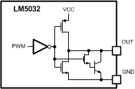 Figure 18. Compound Gate Driver
7.3.11 Thermal Shutdown
The LM5032 should be operated so the junction temperature does not exceed 125°C. If a junction temperature transient reaches 165°C (typical), the Thermal Shutdown circuit activates the VCC Disable and Drivers Off lines (see Figure 14). The VCC regulator and the four output drivers are disabled, the SS1, SS2, and RES pins are grounded, and the soft-start current is set to 50 µA. This puts the LM5032 in a low power state helping to prevent catastrophic failures from accidental device overheating. When the junction temperature reduces below 145°C (typical hysteresis = 20°C), the VCC regulator is enabled and a startup sequence is initiated (Figure 1).
7.4 Device Functional Modes
Normal device operating mode is described above in sections Line Undervoltage Lock Out, UVLO, Shutdown through Cycle-by-Cycle Current Limit, and sections Soft-Start to Thermal Shutdown. Under overcurrent fault conditions, the device operate in Hiccup Mode, as detailed above in the Hiccup Mode Current Limit Restart section.