SNVSB14C April 2018 – October 2021 LM5036
PRODUCTION DATA
- 1 Features
- 2 Applications
- 3 Description
- 4 Revision History
- 5 Pin Configuration and Functions
- 6 Specifications
-
7 Detailed Description
- 7.1 Overview
- 7.2 Functional Block Diagram
- 7.3
Feature Description
- 7.3.1 High-Voltage Start-Up Regulator
- 7.3.2 Undervoltage Lockout (UVLO)
- 7.3.3 Reference Regulator
- 7.3.4 Oscillator, Synchronized Input
- 7.3.5 Voltage-Mode Control
- 7.3.6 Primary-Side Gate Driver Outputs (LSG and HSG)
- 7.3.7 Half-Bridge PWM Scheme
- 7.3.8 Maximum Duty Cycle Operation
- 7.3.9 Pre-Biased Start-Up Process
- 7.3.10 Zero Duty Cycle Operation
- 7.3.11 Enhanced Cycle-by-Cycle Current Limiting with Pulse Matching
- 7.3.12 Reverse Current Protection
- 7.3.13 CBC Threshold Accuracy
- 7.3.14 Hiccup Mode Protection
- 7.3.15 Hiccup Mode Blanking
- 7.3.16 Over-Temperature Protection (OTP)
- 7.3.17 Over-Voltage / Latch (ON_OFF Pin)
- 7.3.18 Auxiliary Constant On-Time Control
- 7.3.19 Auxiliary On-Time Generator
- 7.3.20 Auxiliary Supply Current Limiting
- 7.3.21 Auxiliary Primary Output Capacitor Ripple
- 7.3.22 Auxiliary Ripple Configuration and Control
- 7.3.23 Asynchronous Mode Operation of Auxiliary Supply
- 7.4 Device Functional Modes
-
8 Application and Implementation
- 8.1 Application Information
- 8.2
Typical Application
- 8.2.1 Design Requirements
- 8.2.2
Detailed Design Procedure
- 8.2.2.1 Custom Design With WEBENCH® Tools
- 8.2.2.2 Input Transient Protection
- 8.2.2.3 Level-Shift Detection Circuit
- 8.2.2.4 Applications with VIN > 100-V
- 8.2.2.5 Applications without Pre-Biased Start-Up Requirement
- 8.2.2.6 UVLO Voltage Divider Selection
- 8.2.2.7 Over Voltage, Latch (ON_OFF Pin) Voltage Divider Selection
- 8.2.2.8 SS Capacitor
- 8.2.2.9 SSSR Capacitor
- 8.2.2.10 Half-Bridge Power Stage Design
- 8.2.2.11 Current Limit
- 8.2.2.12 Auxiliary Transformer
- 8.2.2.13 Auxiliary Feedback Resistors
- 8.2.2.14 RON Resistor
- 8.2.2.15 VIN Pin Capacitor
- 8.2.2.16 Auxiliary Primary Output Capacitor
- 8.2.2.17 Auxiliary Secondary Output Capacitor
- 8.2.2.18 Auxiliary Feedback Ripple Circuit
- 8.2.2.19 Auxiliary Secondary Diode
- 8.2.2.20 VCC Diode
- 8.2.2.21 Opto-Coupler Interface
- 8.2.2.22 Full-Bridge Converter Applications
- 8.2.3 Application Curves
- 9 Power Supply Recommendations
- 10Layout
- 11Device and Documentation Support
- 12Mechanical, Packaging, and Orderable Information
Package Options
Mechanical Data (Package|Pins)
- RJB|28
Thermal pad, mechanical data (Package|Pins)
Orderable Information
7.3.7 Half-Bridge PWM Scheme
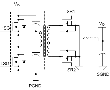
Synchronous rectification on the secondary side of the transformer provides higher efficiency, especially for low output voltage and high output current converter, compared to the diode rectification. The reduction of the diode forward voltage drop (0.5-V to 1.5-V) to 10-mV to 200-mV VDS voltage for a MOSFET significantly reduces rectification losses. In a typical application, the secondary windings of the transformer can be center tapped, with the output power inductor in series with the center tap, as shown in Figure 7-5. The synchronous rectifiers (SRs) provide the ground path for the energized secondary winding and the inductor current.
 Figure 7-5 Half-bridge Topology with Center-Tap Rectification
The internal SR drivers are powered by the REF regulator and each SR output is capable of sourcing 0.1-A and sinking 0.2-A peak (typical). The amplitude of the SR drivers is limited to 5-V. The 5-V SR signals enable the transfer of SR control signals across the isolation barrier either through a digital isolator or isolated gate driver. It should be noted that the actual gate sourcing and sinking currents for the SRs are provided by the secondary-side gate drivers.
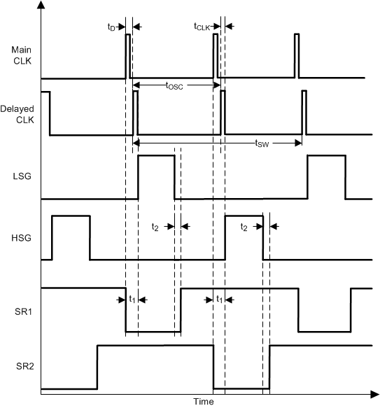
The timing diagram of the four PMW signals (LSG, HSG, SR1, and SR2) with dead-times is illustrated in Figure 7-6. The main clock is generated by the internal oscillator. A delayed clock is derived by adding a delay of tD to the main clock. tD can be calculated from Equation 3, where RD1 is the value of the resistor connected between RD1 pin and AGND.

 Figure 7-6 PWM Signal Timing Diagram
As illustrated in Figure 7-6, the rising edge of the main clock is used to turn off the SRs. Primary FET drive signal LSG/HSG is turned on at the falling edge of the delayed clock. Therefore, the dead-time between the falling edge of SR and the rising edge of the respective primary FET can be calculated from Equation 4

where
- tCLK is the pulse width of the clock which is 65 ns (typical).
The minimum achievable t1 is dominated by the pulse width of the clock when tD is set to minimum (30 ns).
After SR1 is turned off, the body diode of SR1 continues to carry about half the inductor current until the primary power raises the drain voltage of the SR1 and reverse biases its body diode. Ideally, dead-time t1 would be set to the minimum time that allows the SR to turn off before the body diode starts conducting.
Power is transferred from the primary to the secondary side when the LSG is turned on. During this power transfer period, the SR2 is still turned on while the SR1 is turned off. The drain voltage of SR1 is twice the voltage of the center tap at this time. Under the normal operation, the LSG is turned off either when the RAMP signal exceeds the COMP signal or at the rising edge of the next delayed clock signal (maximum duty cycle condition), whichever comes earlier. A dead-time t2 is inserted between the falling edge of LSG and rising edge of SR1. t2 can be calculated from Equation 5, where RD2 is the value of the resistor connected between RD2 pin and AGND.

During the dead-time t2, the inductor current continues to flow through the body diode of SR1. Because the body diode causes more conduction loss than the SR, efficiency can be improved by minimizing the t2 period while maintaining sufficient margin across the entire operating conditions (component tolerances, input voltages, etc.) to prevent the cross conduction between the primary FET and SR.
During the freewheeling period where both of the primary FETs are turned off while both of the SRs are turned on, the inductor current is almost equally shared between SR1 and SR2 which effectively shorts the secondary winding of the transformer. SR2 is then turned off before HSG is turned on. The power is transferred from the primary to secondary side again when HSG is turned on. After HSG is disabled and the dead-time t2 expires, SR1 and SR2 both conduct again during the freewheeling period.
Resistor values of no less than 5-kΩ should be connected between the RD1/RD2 pins and AGND