SNVS703H February 2011 – November 2014 LM5046
PRODUCTION DATA.
- 1 Features
- 2 Applications
- 3 Description
- 4 Revision History
- 5 Pin Configuration and Functions
- 6 Specifications
-
7 Detailed Description
- 7.1 Overview
- 7.2 Functional Block Diagram
- 7.3
Feature Description
- 7.3.1 High-Voltage Start-Up Regulator
- 7.3.2 Line Undervoltage Detector
- 7.3.3 Overvoltage Protection
- 7.3.4 Reference
- 7.3.5 Oscillator, Sync Input
- 7.3.6 Cycle-by-Cycle Current Limit
- 7.3.7 Hiccup Mode
- 7.3.8 PWM Comparator
- 7.3.9 RAMP Pin
- 7.3.10 Slope Pin
- 7.3.11 Soft-Start
- 7.3.12 Gate Driver Outputs
- 7.3.13 Synchronous Rectifier Control Outputs (SR1 & SR2)
- 7.3.14 Soft-Start of the Synchronous Rectifiers
- 7.3.15 Pre-Bias Startup
- 7.3.16 Soft-Stop
- 7.3.17 Soft-Stop Off
- 7.3.18 Thermal Protection
- 7.4 Device Functional Modes
-
8 Application and Implementation
- 8.1 Application Information
- 8.2
Typical Application
- 8.2.1 Design Requirements
- 8.2.2
Detailed Design Procedure
- 8.2.2.1 Phase-Shifted Full-Bridge Operation
- 8.2.2.2 Control Method Selection
- 8.2.2.3 Voltage Mode Control Using the LM5046
- 8.2.2.4 Current Mode Control Using the LM5046
- 8.2.2.5 VIN and VCC
- 8.2.2.6 For Applications With > 100 V Input
- 8.2.2.7 UVLO and OVP Voltage Divider Selection
- 8.2.2.8 Current Sense
- 8.2.2.9 Hiccup Mode Current Limit Restart
- 8.2.2.10 Augmenting the Gate Drive Strength
- 8.2.3 Application Curve
- 9 Power Supply Recommendations
- 10Layout
- 11Device and Documentation Support
- 12Mechanical, Packaging, and Orderable Information
Package Options
Mechanical Data (Package|Pins)
Thermal pad, mechanical data (Package|Pins)
- PWP|28
Orderable Information
10 Layout
10.1 Layout Guidelines
The LM5046 current sense and PWM comparators are very fast and respond to short duration noise pulses. The components at the CS, COMP, SLOPE, RAMP, SS, SSSR, RES, UVLO, OVP, RD1, RD2, and RT pins should be physically close as possible to the IC, thereby minimizing noise pickup on the PC board trace inductance. Eliminating or minimizing via’s in these critical connections are essential. Layout consideration is critical for the current sense filter. If a current sense transformer is used, both leads of the transformer secondary should be routed to the sense filter components and to the IC pins. The ground side of the transformer should be connected via a dedicated PC board trace to the AGND pin, rather than through the ground plane. If the current sense circuit employs a sense resistor in the drive transistor source, low inductance resistors should be used. In this case, all the noise sensitive, low-current ground trace should be connected in common near the IC, and then a single connection made to the power ground (sense resistor ground point).
The gate drive outputs of the LM5046 should have short, direct paths to the power MOSFETs in order to minimize inductance in the PC board. The boot-strap capacitors required for the high side gate drivers should be located very close to the IC and connected directly to the BST and HS pins. The VCC and REF capacitors should also be placed close to their respective pins with short trace inductance. Low ESR and ESL ceramic capacitors are recommended for the boot-strap, VCC and the REF capacitors. The two ground pins (AGND, PGND) must be connected together directly underneath the IC with a short, direct connection, to avoid jitter due to relative ground bounce.
10.2 Layout Example
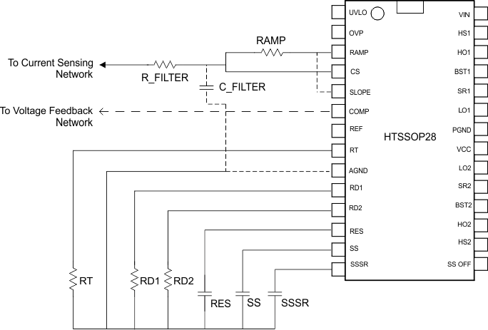 Figure 38. Layout of Components Around RAMP, CS, SLOPE, COMP, RT, RD1, RD2, RES, SS, and SSR
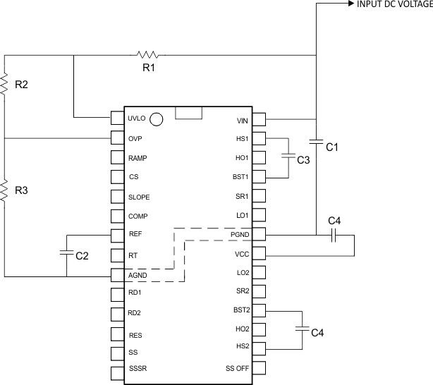 Figure 39. Layout of Components Around VIN, VCC, AGND, PGND UVLO, OVP, REF, BST1, BST2, HS1, and HS2