SNVS703H February 2011 – November 2014 LM5046
PRODUCTION DATA.
- 1 Features
- 2 Applications
- 3 Description
- 4 Revision History
- 5 Pin Configuration and Functions
- 6 Specifications
-
7 Detailed Description
- 7.1 Overview
- 7.2 Functional Block Diagram
- 7.3
Feature Description
- 7.3.1 High-Voltage Start-Up Regulator
- 7.3.2 Line Undervoltage Detector
- 7.3.3 Overvoltage Protection
- 7.3.4 Reference
- 7.3.5 Oscillator, Sync Input
- 7.3.6 Cycle-by-Cycle Current Limit
- 7.3.7 Hiccup Mode
- 7.3.8 PWM Comparator
- 7.3.9 RAMP Pin
- 7.3.10 Slope Pin
- 7.3.11 Soft-Start
- 7.3.12 Gate Driver Outputs
- 7.3.13 Synchronous Rectifier Control Outputs (SR1 & SR2)
- 7.3.14 Soft-Start of the Synchronous Rectifiers
- 7.3.15 Pre-Bias Startup
- 7.3.16 Soft-Stop
- 7.3.17 Soft-Stop Off
- 7.3.18 Thermal Protection
- 7.4 Device Functional Modes
-
8 Application and Implementation
- 8.1 Application Information
- 8.2
Typical Application
- 8.2.1 Design Requirements
- 8.2.2
Detailed Design Procedure
- 8.2.2.1 Phase-Shifted Full-Bridge Operation
- 8.2.2.2 Control Method Selection
- 8.2.2.3 Voltage Mode Control Using the LM5046
- 8.2.2.4 Current Mode Control Using the LM5046
- 8.2.2.5 VIN and VCC
- 8.2.2.6 For Applications With > 100 V Input
- 8.2.2.7 UVLO and OVP Voltage Divider Selection
- 8.2.2.8 Current Sense
- 8.2.2.9 Hiccup Mode Current Limit Restart
- 8.2.2.10 Augmenting the Gate Drive Strength
- 8.2.3 Application Curve
- 9 Power Supply Recommendations
- 10Layout
- 11Device and Documentation Support
- 12Mechanical, Packaging, and Orderable Information
Package Options
Mechanical Data (Package|Pins)
Thermal pad, mechanical data (Package|Pins)
- PWP|28
Orderable Information
6 Specifications
6.1 Absolute Maximum Ratings(1)
| MIN | MAX | UNIT | |
|---|---|---|---|
| VIN to GND | –0.3 | 105 | V |
| HS to GND(2) | –5 | 105 | V |
| BST1/BST2 to GND | –0.3 | 116 | V |
| BST1/BST2 to HS1/HS2 | –0.3 | 16 | V |
| HO1/HO2 to HS1/HS2(1) | –0.3 | BST1/BST2+0.3 | V |
| LO1/LO2/SR1/SR2(1) | –0.3 | VCC+0.3 | V |
| VCC to GND | –0.3 | 16 | V |
| REF,SSOFF,RT,OVP,UVLO to GND | –0.3 | 7 | V |
| RAMP | –0.3 | 7 | V |
| COMP | –0.3 | V | |
| COMP Input Current | 10 | mA | |
| All other inputs to GND(1) | –0.3 | REF+0.3 | V |
| Junction Temperature | 150 | °C |
(1) Absolute Maximum Ratings are limits beyond which damage to the device may occur. Operating Ratings are conditions under which operation of the device is intended to be functional. For specifications and test conditions, see Electrical Characteristics.
6.2 Handling Ratings
| MIN | MAX | UNIT | |||
|---|---|---|---|---|---|
| Tstg | Storage temperature range | –55 | 150 | °C | |
| V(ESD) | Electrostatic discharge | Human body model (HBM), per ANSI/ESDA/JEDEC JS-001, all pins(1) | 2 | kV | |
| Charged device model (CDM), per JEDEC specification JESD22-C101, all pins(2) | 750 | V | |||
(1) JEDEC document JEP155 states that 500-V HBM allows safe manufacturing with a standard ESD control process.
(2) JEDEC document JEP157 states that 250-V CDM allows safe manufacturing with a standard ESD control process.
6.3 Recommended Operating Conditions
over operating free-air temperature range (unless otherwise noted)| MIN | MAX | UNIT | |
|---|---|---|---|
| VIN Voltage | 14 | 100 | V |
| External Voltage Applied to VCC | 10 | 14 | V |
| Junction Temperature | –40 | 125 | °C |
| SLOPE | –0.3 | 2 | V |
6.4 Thermal Information
| THERMAL METRIC(1) | LM5046 | UNIT | ||
|---|---|---|---|---|
| PWP | RSG | |||
| 28 PINS | ||||
| RθJA | Junction-to-ambient thermal resistance | 33.9 | 37.4 | °C/W |
| RθJC(top) | Junction-to-case (top) thermal resistance | 18.1 | 21.8 | |
| RθJB | Junction-to-board thermal resistance | 15.7 | 10.1 | |
| ψJT | Junction-to-top characterization parameter | 0.4 | 0.2 | |
| ψJB | Junction-to-board characterization parameter | 15.6 | 10 | |
| RθJC(bot) | Junction-to-case (bottom) thermal resistance | 2.0 | 2.6 | |
(1) For more information about traditional and new thermal metrics, see the IC Package Thermal Metrics application report, SPRA953.
6.5 Electrical Characteristics
Limits in standard typeface are for TJ = 25°C only; for the MIN and MAX apply the junction temperature range of –40°C to 125°C. Unless otherwise specified, the following conditions apply: VIN = 48 V, RT = 25 kΩ, RD1 = RD2 = 20 kΩ. No load on HO1, HO2, LO1, LO2, SR1, SR2, COMP=0 V, UVLO = 2.5 V, OVP = 0 V, SSOFF = 0 V.| PARAMETER | TEST CONDITIONS | MIN | TYP | MAX | UNIT | |
|---|---|---|---|---|---|---|
| STARTUP REGULATOR (VCC PIN) | ||||||
| VCC1 | VCC voltage | ICC= 10 mA (SSSR < 1 V) | 9.3 | 9.6 | 9.9 | V |
| VCC2 | VCC voltage | ICC= 10 mA (SSSR > 1 V) | 7.5 | 7.8 | 8.1 | V |
| ICC(Lim) | VCC current limit | VCC= 6 V | 60 | 80 | mA | |
| ICC(ext) | VCC supply current | Supply current into VCC from an externally applied source. VCC = 10 V | 4.6 | mA | ||
| VCC load regulation | ICC from 0 to 50 mA | 35 | mV | |||
| VCC(UV) | VCC under-voltage threshold | Positive going VCC | VCC1–0.2 | VCC1–0.1 | V | |
| VCC under-voltage threshold | Negative going VCC | 5.9 | 6.3 | 6.7 | V | |
| IIN | VIN operating current | 4 | mA | |||
| VIN shutdown current | VIN = 20 V, VUVLO = 0 V | 300 | 520 | µA | ||
| VVIN = 100 V, VUVLO = 0 V | 350 | 550 | µA | |||
| VIN start-up regulator leakage | VCC = 10 V | 160 | µA | |||
| VOLTAGE REFERENCE REGULATOR (REF PIN) | ||||||
| VREF | REF Voltage | IREF = 0 mA | 4.85 | 5 | 5.15 | V |
| REF voltage regulation | IREF = 0 to 10 mA | 25 | 50 | mV | ||
| IREF(Lim) | REF current limit | VREF = 4.5 V | 15 | 20 | mA | |
| VREFUV | VREF under-voltage threshold | Positive going VREF | 4.3 | 4.5 | 4.7 | V |
| Hysteresis | 0.25 | V | ||||
| UNDERVOLTAGE LOCK OUT AND SHUTDOWN (UVLO PIN) | ||||||
| VUVLO | Under-voltage threshold | 1.18 | 1.25 | 1.32 | V | |
| IUVLO | Hysteresis current | UVLO pin sinking current when VUVLO < 1.25 V | 16 | 20 | 24 | µA |
| Under-voltage standby enable threshold | UVLO voltage rising | 0.32 | 0.4 | 0.48 | V | |
| Hysteresis | 0.05 | V | ||||
| VOVP | OVP shutdown threshold | OVP rising | 1.18 | 1.25 | 1.32 | V |
| OVP hysteresis current | OVP sources current when OVP > 1.25 V | 16 | 20 | 24 | µA | |
| SOFT-START (SS PIN) | ||||||
| ISS | SS charge current | VSS = 0 V | 16 | 20 | 24 | µA |
| SS threshold for SSSR charge current enable | ICOMP < 800 µA | 1.93 | 2.0 | 2.20 | V | |
| SS output low voltage | Sinking 100 µA | 40 | mV | |||
| SS threshold to disable switching | 200 | mV | ||||
| ISSSR | SSSR charge current | VSS > 2 V, ICOMP < 800 µA | 16 | 20 | 24 | µA |
| ISSSR-DIS1 | SSSR discharge current 1 | VUVLO < 1.25 V | 54 | 65 | 75 | µA |
| ISSSR-DIS2 | SSSR discharge current 2 | VRES > 1 V | 109 | 125 | 147 | µA |
| SSSR output low voltage | Sinking 100 µA | 50 | mV | |||
| SSSR threshold to enable SR1/SR2 | 1.2 | V | ||||
| CURRENT SENSE INPUT (CS PIN) | ||||||
| VCS | Current limit threshold | 0.710 | 0.750 | 0.785 | V | |
| CS delay to output | 65 | ns | ||||
| CS leading edge blanking | 50 | ns | ||||
| RCS | CS sink impedance (clocked) | Internal FET sink impedance | 18 | 45 | Ω | |
| SOFT-STOP DISABLE (SS OFF PIN) | ||||||
| VIH(min) | SSOFF Input Threshold | 2.8 | V | |||
| SSOFF pull down resistance | 200 | kΩ | ||||
| CURRENT LIMIT RESTART (RES PIN) | ||||||
| RRES | RES pull-down resistance | Termination of hiccup timer | 37 | Ω | ||
| VRES | RES hiccup threshold | 1 | V | |||
| RES upper counter threshold | 4 | V | ||||
| RES lower counter threshold | 2 | V | ||||
| IRES-SRC1 | Charge current source 1 | VRES < 1 V, VCS> 750 mV | 30 | µA | ||
| IRES-SRC2 | Charge current source 2 | 1 V < VRES < 4 V | 10 | µA | ||
| IRES-DIS2 | Discharge current source 1 | VCS < 750 mV | 5 | µA | ||
| IRES-DIS2 | Discharge current source 2 | 2 V < VRES < 4 V | 5 | µA | ||
| Ratio of time in hiccup mode to time in current limit | VRES > 1 V, Hiccup counter | 147 | ||||
| VOLTAGE FEED-FORWARD (RAMP PIN) | ||||||
| RAMP sink impedance (Clocked) | 5.5 | 20 | Ω | |||
| OSCILLATOR (RT PIN) | ||||||
| FSW1 | Frequency (LO1, half oscillator frequency) | RT = 25 kΩ | 185 | 200 | 215 | kHz |
| FSW2 | Frequency (LO1, half oscillator frequency) | RT = 10 kΩ | 420 | 480 | 540 | kHz |
| DC level | 2.0 | V | ||||
| RT sync threshold | 2.8 | 3 | 3.3 | V | ||
| ZVS TIMING CONTROL (RD1 & RD2 PINS) | ||||||
| TPA | HO1/SR1 turn-off to LO1 turn-on LO1/SR2 turn-off to HO1 turn-on |
RD1 = 20 kΩ | 39 | 65 | 89 | ns |
| RD1 = 100 kΩ | 230 | 300 | 391 | ns | ||
| TAP | LO2 turn-off to HO2 turn-on HO2 turn-off to LO2 turn-on |
RD2 = 20 kΩ | 27 | 55 | 78 | ns |
| RD2 = 100 kΩ | 214 | 300 | 378 | ns | ||
| COMP PIN | ||||||
| VPWM-OS | COMP current to RAMP offset | VRAMP = 0 V | 680 | 800 | 940 | µA |
| VSS-OS | SS to RAMP offset | VRAMP = 0 V | 0.78 | 1.0 | 1.22 | V |
| COMP current to RAMP gain | ΔRAMP/ΔICOMP | 2400 | Ω | |||
| SS to RAMP gain | ΔSS/ΔRAMP | 0.5 | ||||
| COMP current for SSSR charge current enable | VSS > 2 V | 690 | 800 | 915 | µA | |
| COMP to output delay | 120 | ns | ||||
| Minimum duty cycle | ICOMP = 1 mA | 0 | % | |||
| SLOPE COMPENSATION (SLOPE PIN) | ||||||
| ISLOPE | Slope compensation current ramp | Peak of RAMP current | 100 | µA | ||
| BOOST (BST PIN) | ||||||
| VBst uv | BST under-voltage threshold | VBST – VHS rising | 3.8 | 4.7 | 5.6 | V |
| Hysteresis | 0.5 | V | ||||
| HO1, HO2, LO1, LO2 GATE DRIVERS | ||||||
| VOL | Low-state output voltage | IHO/LO = 100 mA | 0.16 | 0.32 | V | |
| VOH | High-state output voltage | IHO/LO = 100 mA VOHL = VCC – VLO VOHH = VBST – VHO |
0.27 | 0.495 | V | |
| Rise Time | C-load = 1000 pF | 16 | ns | |||
| Fall Time | C-load = 1000 pF | 11 | ns | |||
| IOHL | Peak Source Current | VHO/LO = 0 V | 1.5 | - | A | |
| IOLL | Peak Sink Current | VHO/LO = VCC | 2 | - | A | |
| SR1, SR2 GATE DRIVERS | ||||||
| VOL | Low-state output voltage | ISR1/SR2 = 10 mA | 0.05 | 0.10 | V | |
| VOH | High-state output voltage | ISR1/SR2 = 10 mA, VOH = VREF – VSR |
0.17 | 0.28 | V | |
| Rise Time | C-load = 1000 pF | 60 | ns | |||
| Fall Time | C-load = 1000 pF | 20 | ns | |||
| IOHL | Peak Source Current | VSR = 0 V | 0.1 | - | A | |
| IOLL | Peak Sink Current | VSR = VREF | 0.4 | - | A | |
| THERMAL | ||||||
| TSD | Thermal Shutdown Temp | 160 | °C | |||
| Thermal Shutdown Hysteresis | 25 | °C | ||||
(1) These pins are output pins and as such should not be connected to an external voltage source. The voltage range listed is the limits the internal circuitry is designed to reliably tolerate in the application circuit.
(2) The negative HS voltage must never be more negative than VCC-16V. For example, if VCC = 12 V, the negative transients at HS must not exceed –4 V.
6.6 Typical Characteristics
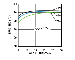 Figure 1. Application Board Efficiency
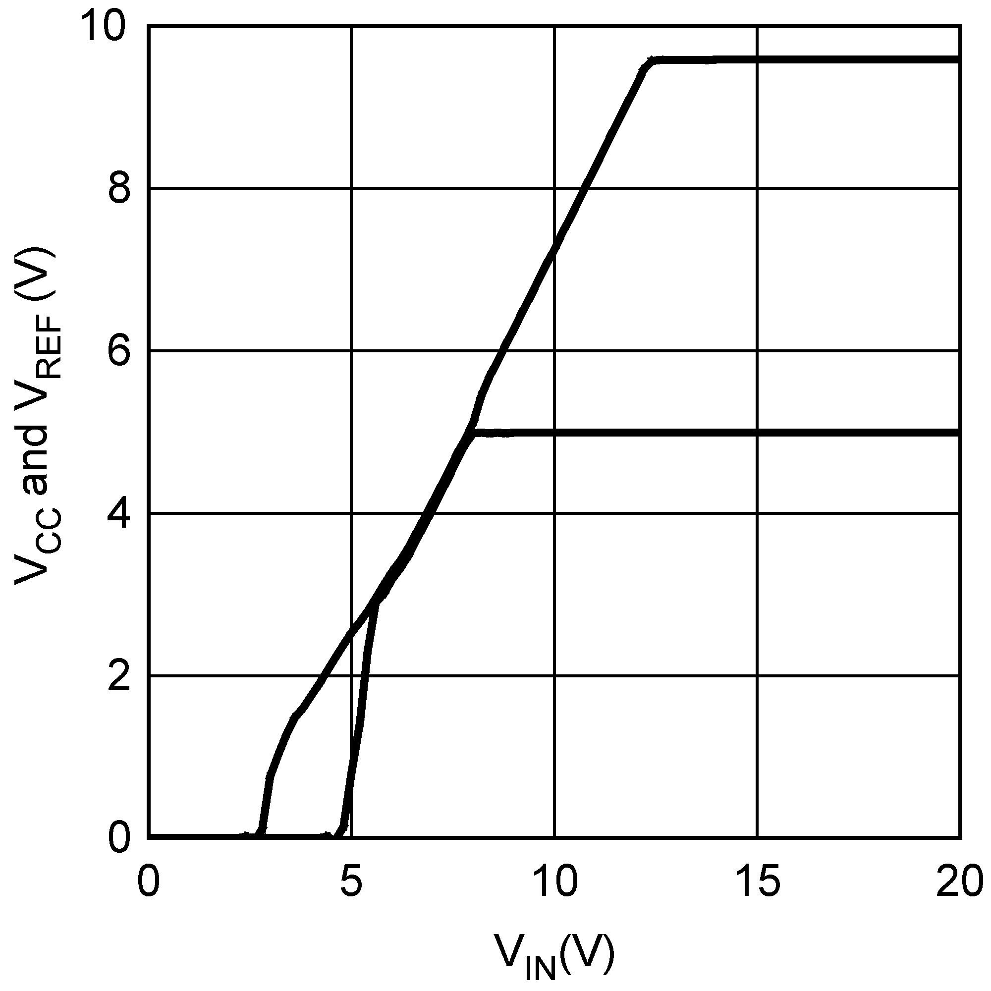 Figure 3. VVCC and VREF vs. VVIN
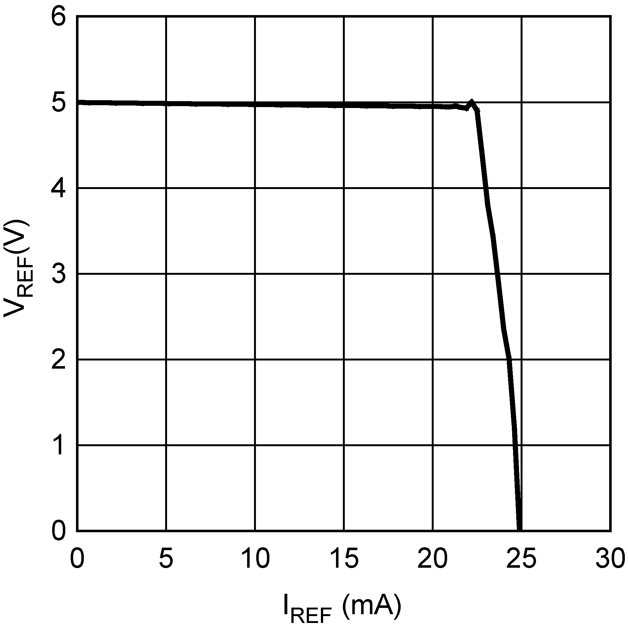 Figure 5. VREF vs. IREF
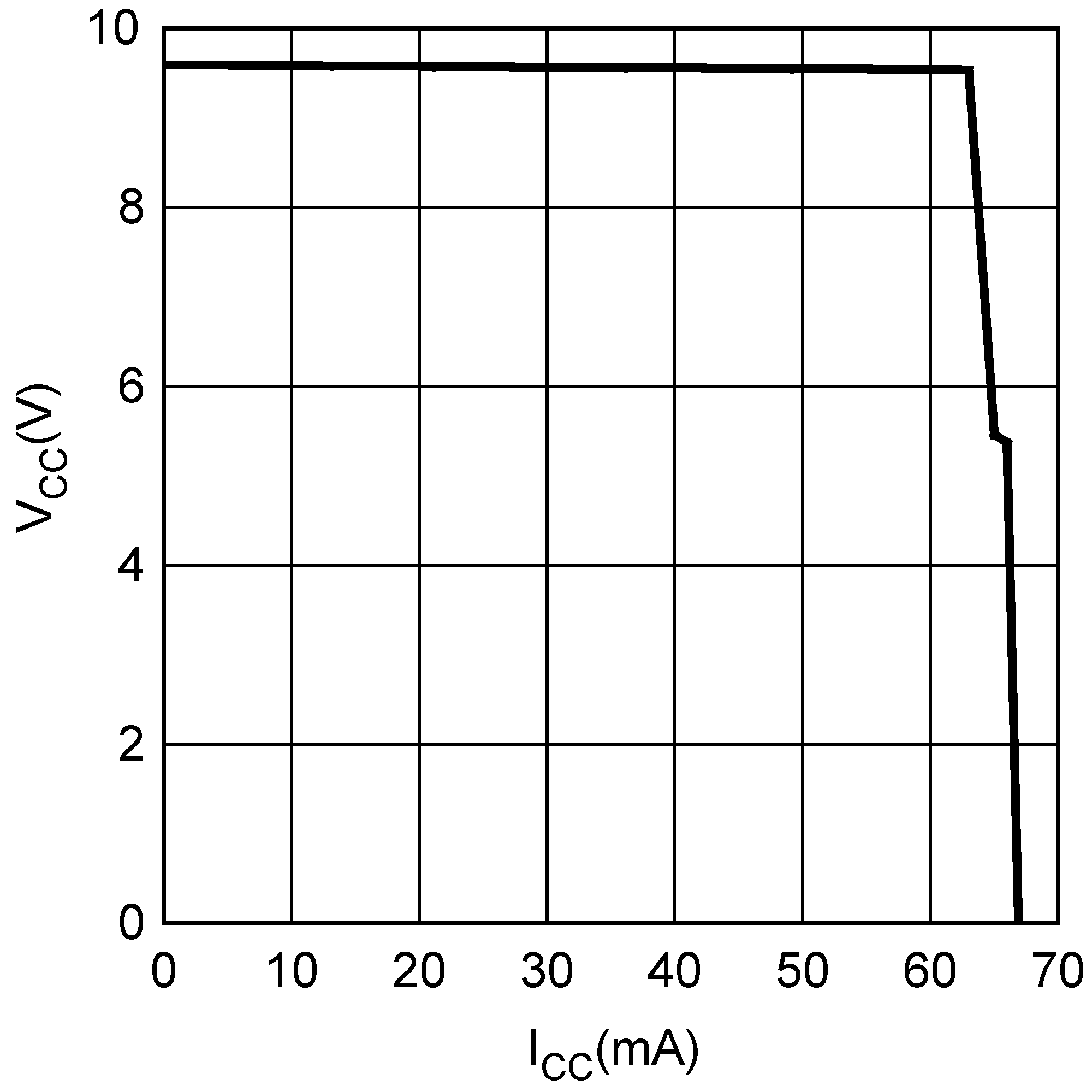 Figure 2. VCC vs ICC
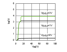 Figure 4. IIN vs. VIN
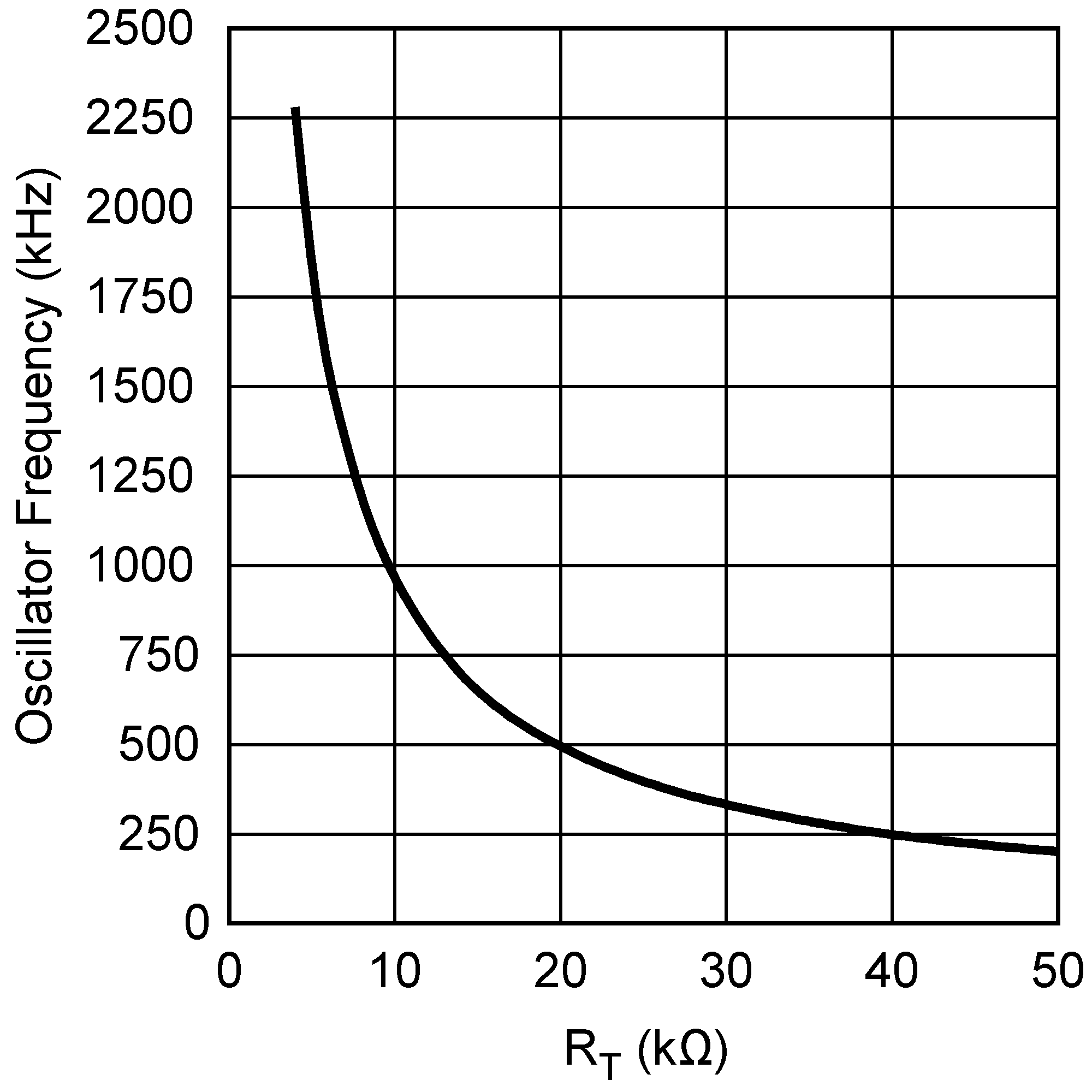 Figure 6. Oscillator Frequency vs. RT
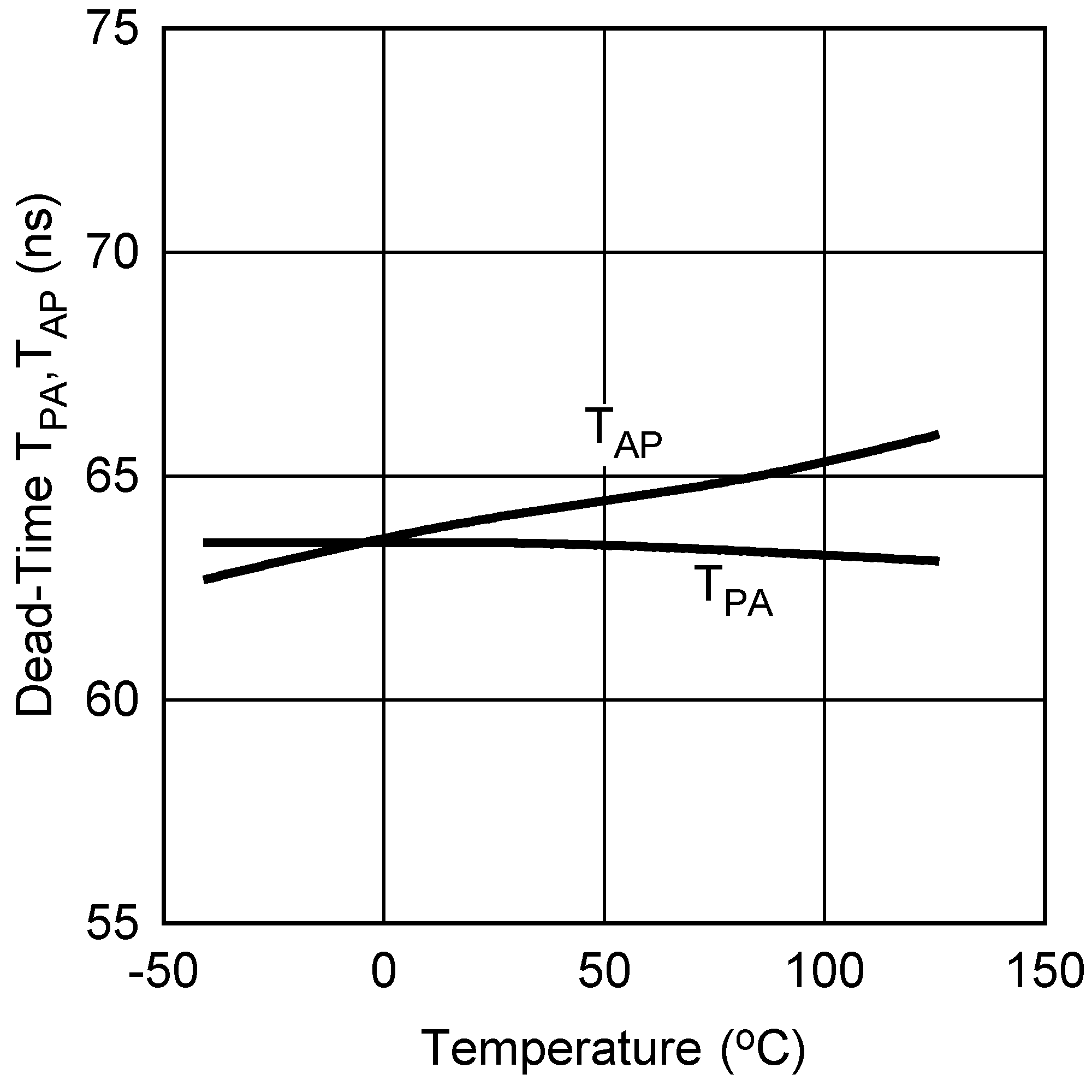 Figure 7. Dead-Time TPA, TAP vs. Temperature
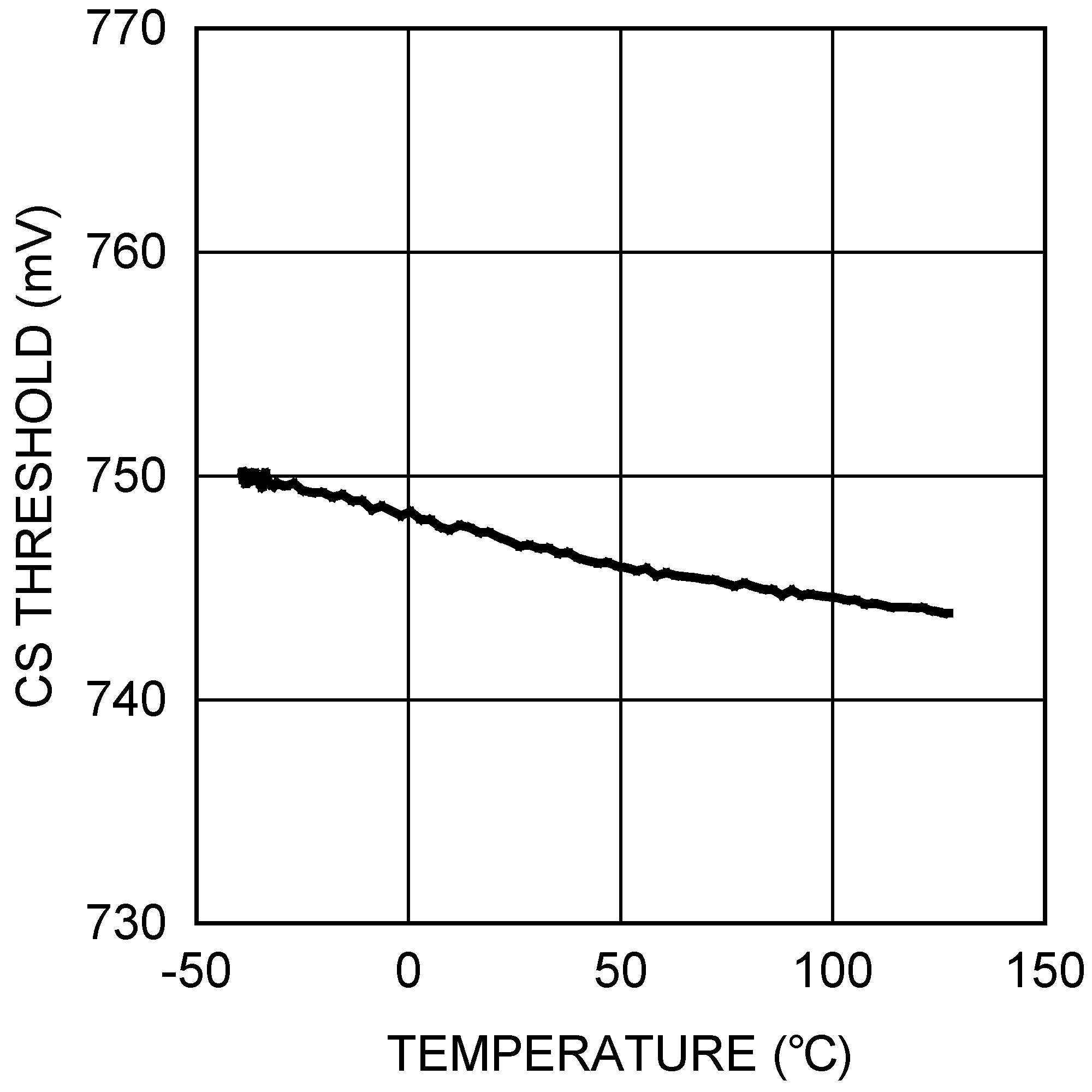 Figure 9. CS Threshold vs. Temperature
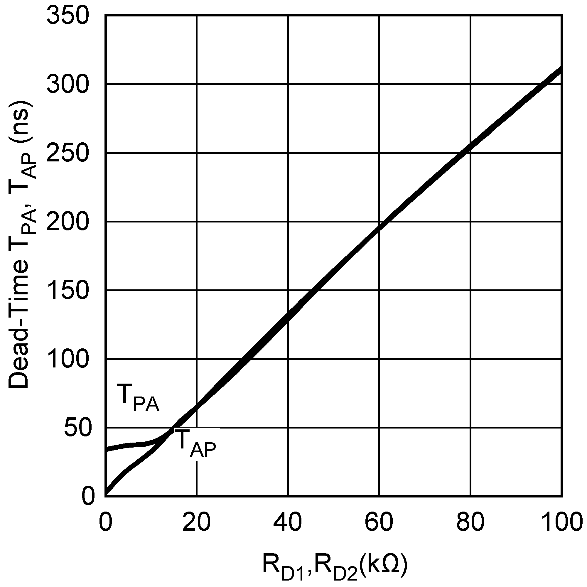 Figure 8. Dead-Time TPA, TAP vs. RD1, RD2