SNVS725I June   2011  – October 2019 LM5113

PRODUCTION DATA.  

  1. Features
  2. Applications
  3. Description
    1.     Device Images
      1.      Simplified Application Diagram
  4. Revision History
  5. Pin Configuration and Functions
    1.     Pin Functions
  6. Specifications
    1. 6.1 Absolute Maximum Ratings
    2. 6.2 ESD Ratings
    3. 6.3 Recommended Operating Conditions
    4. 6.4 Thermal Information
    5. 6.5 Electrical Characteristics
    6. 6.6 Switching Characteristics
    7. 6.7 Typical Characteristics
  7. Detailed Description
    1. 7.1 Overview
    2. 7.2 Functional Block Diagram
    3. 7.3 Feature Description
      1. 7.3.1 Input and Output
      2. 7.3.2 Start-Up and UVLO
      3. 7.3.3 HS Negative Voltage and Bootstrap Supply Voltage Clamping
      4. 7.3.4 Level Shift
    4. 7.4 Device Functional Modes
  8. Application and Implementation
    1. 8.1 Application Information
    2. 8.2 Typical Application
      1. 8.2.1 Design Requirements
      2. 8.2.2 Detailed Design Procedure
        1. 8.2.2.1 VDD Bypass Capacitor
        2. 8.2.2.2 Bootstrap Capacitor
        3. 8.2.2.3 Power Dissipation
      3. 8.2.3 Application Curves
  9. Power Supply Recommendations
  10. 10Layout
    1. 10.1 Layout Guidelines
    2. 10.2 Layout Examples
  11. 11Device and Documentation Support
    1. 11.1 Documentation Support
      1. 11.1.1 Related Documentation
    2. 11.2 Support Resources
    3. 11.3 Trademarks
    4. 11.4 Electrostatic Discharge Caution
    5. 11.5 Glossary
  12. 12Mechanical, Packaging, and Orderable Information

Package Options

Mechanical Data (Package|Pins)
Thermal pad, mechanical data (Package|Pins)
Orderable Information

Typical Application

The circuit in Figure 18 shows a synchronous buck converter to evaluate LM5113. Detailed synchronous buck converter specifications are listed in Design Requirements. The active clamping voltage mode controller LM5025 is used for close-loop control and generates the PWM signals of the buck switch and the synchronous switch. For more information, refer to the Related Documentation section.
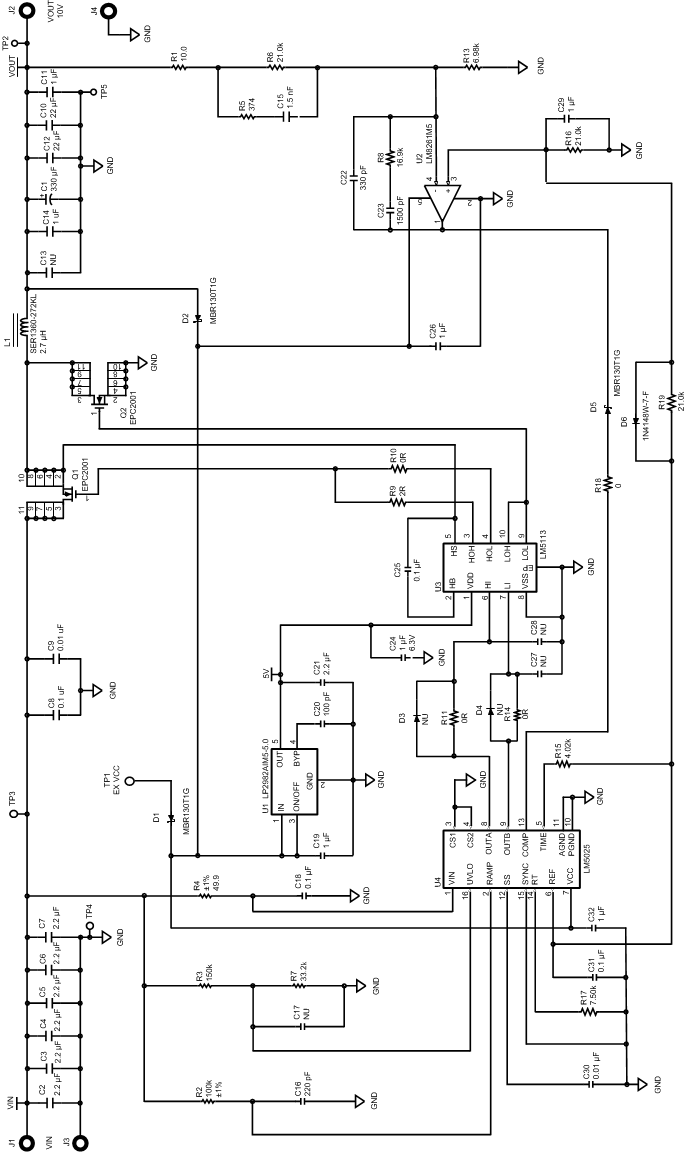
LM5113 30163008.gif
Input 15 V to 60 V, output 10 V, 800 kHz
Figure 18. Application Circuit