SNVSB75E december 2018 – august 2023 LM5155 , LM51551
PRODUCTION DATA
- 1
- 1 Features
- 2 Applications
- 3 Description
- 4 Revision History
- 5 Description (continued)
- 6 Device Comparison Table
- 7 Pin Configuration and Functions
- 8 Specifications
-
9 Detailed Description
- 9.1 Overview
- 9.2 Functional Block Diagram
- 9.3
Feature Description
- 9.3.1 Line Undervoltage Lockout (UVLO/SYNC Pin)
- 9.3.2 High Voltage VCC Regulator (BIAS, VCC Pin)
- 9.3.3 Soft Start (SS Pin)
- 9.3.4 Switching Frequency (RT Pin)
- 9.3.5 Clock Synchronization (UVLO/SYNC Pin)
- 9.3.6 Current Sense and Slope Compensation (CS Pin)
- 9.3.7 Current Limit and Minimum On-time (CS Pin)
- 9.3.8 Feedback and Error Amplifier (FB, COMP Pin)
- 9.3.9 Power-Good Indicator (PGOOD Pin)
- 9.3.10 Hiccup Mode Overload Protection (LM51551 Only)
- 9.3.11 Maximum Duty Cycle Limit and Minimum Input Supply Voltage
- 9.3.12 MOSFET Driver (GATE Pin)
- 9.3.13 Overvoltage Protection (OVP)
- 9.3.14 Thermal Shutdown (TSD)
- 9.4 Device Functional Modes
- 10Application and Implementation
- 11Device and Documentation Support
- 12Mechanical, Packaging, and Orderable Information
Package Options
Mechanical Data (Package|Pins)
- DSS|12
Thermal pad, mechanical data (Package|Pins)
- DSS|12
Orderable Information
3 Description
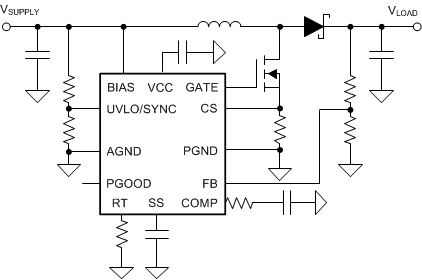
The LM5155x (LM5155 and LM51551) is a wide input range, non-synchronous boost controller that uses peak current mode control. The device can be used in boost, SEPIC, and flyback topologies.
The LM5155x can start up from a 1-cell battery with a minimum of 2.97 V if the BIAS pin is connected to the VCC pin. It can operate with the input supply voltage as low as 1.5 V if the BIAS pin is greater than 3.5 V.
Device
Information
| PART NUMBER | PACKAGE (1) | BODY SIZE (NOM) |
|---|---|---|
| LM5155x | WSON (12) | 3.00 mm × 2.00 mm |
(1) For all available packages, see the orderable addendum at the end of the data sheet.
 Typical Boost Application