SNVSB75E december 2018 – august 2023 LM5155 , LM51551
PRODUCTION DATA
- 1
- 1 Features
- 2 Applications
- 3 Description
- 4 Revision History
- 5 Description (continued)
- 6 Device Comparison Table
- 7 Pin Configuration and Functions
- 8 Specifications
-
9 Detailed Description
- 9.1 Overview
- 9.2 Functional Block Diagram
- 9.3
Feature Description
- 9.3.1 Line Undervoltage Lockout (UVLO/SYNC Pin)
- 9.3.2 High Voltage VCC Regulator (BIAS, VCC Pin)
- 9.3.3 Soft Start (SS Pin)
- 9.3.4 Switching Frequency (RT Pin)
- 9.3.5 Clock Synchronization (UVLO/SYNC Pin)
- 9.3.6 Current Sense and Slope Compensation (CS Pin)
- 9.3.7 Current Limit and Minimum On-time (CS Pin)
- 9.3.8 Feedback and Error Amplifier (FB, COMP Pin)
- 9.3.9 Power-Good Indicator (PGOOD Pin)
- 9.3.10 Hiccup Mode Overload Protection (LM51551 Only)
- 9.3.11 Maximum Duty Cycle Limit and Minimum Input Supply Voltage
- 9.3.12 MOSFET Driver (GATE Pin)
- 9.3.13 Overvoltage Protection (OVP)
- 9.3.14 Thermal Shutdown (TSD)
- 9.4 Device Functional Modes
- 10Application and Implementation
- 11Device and Documentation Support
- 12Mechanical, Packaging, and Orderable Information
Package Options
Mechanical Data (Package|Pins)
- DSS|12
Thermal pad, mechanical data (Package|Pins)
- DSS|12
Orderable Information
9.3.7 Current Limit and Minimum On-time (CS Pin)
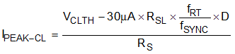
The device provides cycle-by-cycle peak current limit protection that turns off the MOSFET when the sum of the inductor current and the programmable slope compensation ramp reaches the current limit threshold (VCLTH). Peak inductor current limit (IPEAK-CL) in steady state is calculated as shown in Equation 10.
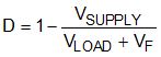
The practical duty cycle is greater than the estimated due to voltage drops across the MOSFET and sense resistor. The estimated duty cycle is calculated as shown in Equation 11.
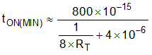
Boost converters have a natural pass-through path from the supply to the load through the high-side power diode (D1). Because of this path and the minimum on-time limitation of the device, boost converters cannot provide current limit protection when the output voltage is close to or less than the input supply voltage. The minimum on-time is shown in Figure 8-12 and is calculated as Equation 12.
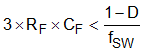
If required, a small external RC filter (RF, CF) at the CS pin can be added to overcome the large leading edge spike of the current sense signal. Select an RF value in the range of 10 Ω to 200 Ω and a CF value in the range of 100 pF to 2 nF. Because of the effect of this RC filter, the peak current limit is not valid when the on-time is less than 2 × RF × CF. To fully discharge the CF during the off-time, the RC time constant should satisfy the following inequality.