SNVSBK7A july 2021 – august 2023 LM5157
PRODUCTION DATA
- 1
- 1 Features
- 2 Applications
- 3 Description
- 4 Revision History
- 5 Device Comparison Table
- 6 Pin Configuration and Functions
- 7 Specifications
-
8 Detailed Description
- 8.1 Overview
- 8.2 Functional Block Diagram
- 8.3
Feature Description
- 8.3.1 Line Undervoltage Lockout (UVLO/SYNC/EN Pin)
- 8.3.2 High Voltage VCC Regulator (BIAS, VCC Pin)
- 8.3.3 Soft Start (SS Pin)
- 8.3.4 Switching Frequency (RT Pin)
- 8.3.5 Dual Random Spread Spectrum – DRSS (MODE Pin)
- 8.3.6 Clock Synchronization (UVLO/SYNC/EN Pin)
- 8.3.7 Current Sense and Slope Compensation
- 8.3.8 Current Limit and Minimum On Time
- 8.3.9 Feedback and Error Amplifier (FB, COMP Pin)
- 8.3.10 Power-Good Indicator (PGOOD Pin)
- 8.3.11 Hiccup Mode Overload Protection (MODE Pin)
- 8.3.12 Maximum Duty Cycle Limit and Minimum Input Supply Voltage
- 8.3.13 Internal MOSFET (SW Pin)
- 8.3.14 Overvoltage Protection (OVP)
- 8.3.15 Thermal Shutdown (TSD)
- 8.4 Device Functional Modes
- 9 Application and Implementation
- 10Power Supply Recommendations
- 11Layout
- 12Device and Documentation Support
- 13Mechanical, Packaging, and Orderable Information
Package Options
Mechanical Data (Package|Pins)
- RTE|16
Thermal pad, mechanical data (Package|Pins)
- RTE|16
Orderable Information
8.3.1 Line Undervoltage Lockout (UVLO/SYNC/EN Pin)
The device has a dual-level EN/UVLO circuit. During power on, if the BIAS pin voltage is greater than 2.7 V and the UVLO pin voltage is between the enable threshold (VEN) and the UVLO threshold (VUVLO) for more than 1.5 µs (see Section 8.3.6 for more details), the device starts up and an internal configuration starts. The device typically requires a 90-µs internal start-up delay before entering Standby mode. In Standby mode, the VCC regulator and RT regulator are operational, the SS pin is grounded, and there is no switching at the SW pin.
 Figure 8-1 Line UVLO and Enable
When the UVLO pin voltage is above the UVLO threshold, the device enters Run mode. In Run mode, a soft-start sequence starts if the VCC voltage is greater than the VCC UV threshold (VVCC-UVLO). UVLO hysteresis is accomplished with an internal 50-mV voltage hysteresis and an additional 5-μA current source that is switched on or off. When the UVLO pin voltage exceeds the UVLO threshold, the UVLO hysteresis current source is enabled to quickly raise the voltage at the UVLO pin. When the UVLO pin voltage falls below the UVLO threshold, the current source is disabled, causing the voltage at the UVLO pin to fall quickly. When the UVLO pin voltage is less than the enable threshold (VEN), the device enters Shutdown mode after a 40-µs (typical) delay with all functions disabled.
 Figure 8-2 Boost Start-Up Waveforms Case 1: Start-Up by VCC UVLO, UVLO Toggle After Start-Up
 Figure 8-3 Boost Start-Up Waveforms Case 2: Start-Up by VCC UVLO, EN Toggle After Start-Up
The external UVLO resistor divider must be designed so that the voltage at the UVLO pin is greater than 1.5 V (typical) when the input voltage is in the desired operating range. The values of RUVLOT and RUVLOB can be calculated as shown in Equation 1 and Equation 2.
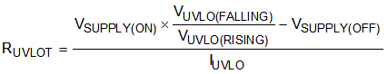
where
- VSUPPLY(ON) is the desired start-up voltage of the converter
- VSUPPLY(OFF) is the desired turn-off voltage of the converter

A UVLO capacitor (CUVLO) is required in case the input voltage drops below the VSUPPLY(OFF) momentarily during start-up or during a severe load transient at the low input voltage. If the required UVLO capacitor is large, an additional series UVLO resistor (RUVLOS) can be used to quickly raise the voltage at the UVLO pin when the 5-μA hysteresis current turns on.
 Figure 8-4 Line UVLO using Three UVLO Resistors
Do not leave the UVLO pin floating. Connect to the BIAS pin if not used.