SNVSBK7A july 2021 – august 2023 LM5157
PRODUCTION DATA
- 1
- 1 Features
- 2 Applications
- 3 Description
- 4 Revision History
- 5 Device Comparison Table
- 6 Pin Configuration and Functions
- 7 Specifications
-
8 Detailed Description
- 8.1 Overview
- 8.2 Functional Block Diagram
- 8.3
Feature Description
- 8.3.1 Line Undervoltage Lockout (UVLO/SYNC/EN Pin)
- 8.3.2 High Voltage VCC Regulator (BIAS, VCC Pin)
- 8.3.3 Soft Start (SS Pin)
- 8.3.4 Switching Frequency (RT Pin)
- 8.3.5 Dual Random Spread Spectrum – DRSS (MODE Pin)
- 8.3.6 Clock Synchronization (UVLO/SYNC/EN Pin)
- 8.3.7 Current Sense and Slope Compensation
- 8.3.8 Current Limit and Minimum On Time
- 8.3.9 Feedback and Error Amplifier (FB, COMP Pin)
- 8.3.10 Power-Good Indicator (PGOOD Pin)
- 8.3.11 Hiccup Mode Overload Protection (MODE Pin)
- 8.3.12 Maximum Duty Cycle Limit and Minimum Input Supply Voltage
- 8.3.13 Internal MOSFET (SW Pin)
- 8.3.14 Overvoltage Protection (OVP)
- 8.3.15 Thermal Shutdown (TSD)
- 8.4 Device Functional Modes
- 9 Application and Implementation
- 10Power Supply Recommendations
- 11Layout
- 12Device and Documentation Support
- 13Mechanical, Packaging, and Orderable Information
Package Options
Mechanical Data (Package|Pins)
- RTE|16
Thermal pad, mechanical data (Package|Pins)
- RTE|16
Orderable Information
3 Description
The LM5157 device is a wide input range, non-synchronous boost converter with integrated 50-V power switch.
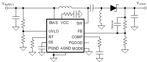
The device can be used in boost, SEPIC, and flyback topologies. The device can start up from a single-cell battery with a minimum of 2.9 V. It can operate with an input supply voltage as low as 1.5 V if the BIAS pin is greater than 2.9 V.
The BIAS pin operates up to 45 V (50-V absolute maximum). The switching frequency is dynamically programmable with an external resistor from 100 kHz to 2.2 MHz. Switching at 2.2 MHz minimizes AM band interference and allows for a small solution size and fast transient response. To reduce the EMI of the power supply, the device provides a selectable Dual Random Spread Spectrum, which reduces the EMI over a wide frequency range.
The device features an accurate peak current limit over the input voltage, which avoids overdesigning power inductor. Low operating current and pulse-skipping operation improve efficiency at light loads.
The device has built-in protection features such as overvoltage protection, line UVLO, thermal shutdown, and selectable Hiccup mode overload protection. Additional features include low shutdown IQ, programmable soft start, precision reference, a power-good indicator, and external clock synchronization.
| PART NUMBER | PACKAGE(1) | BODY SIZE (NOM) |
|---|---|---|
| LM5157 | WQFN (16) | 3.00 mm × 3.00 mm |
 Typical Sepic Application