SNVSAE3B March 2016 – November 2017 LM5161
PRODUCTION DATA.
- 1 Features
- 2 Applications
- 3 Description
- 4 Revision History
- 5 Pin Configuration and Functions
- 6 Specifications
-
7 Detailed Description
- 7.1 Overview
- 7.2 Functional Block Diagram
- 7.3
Feature Description
- 7.3.1 Control Circuit
- 7.3.2 VCC Regulator
- 7.3.3 Regulation Comparator
- 7.3.4 Soft-Start
- 7.3.5 Error Transconductance (GM) Amplifier
- 7.3.6 On-Time Generator
- 7.3.7 Current Limit
- 7.3.8 N-Channel Buck Switch and Driver
- 7.3.9 Synchronous Rectifier
- 7.3.10 Enable / Undervoltage Lockout (EN/UVLO)
- 7.3.11 Thermal Protection
- 7.4 Device Functional Modes
-
8 Applications and Implementation
- 8.1 Application Information
- 8.2
Typical Applications
- 8.2.1
LM5161 Synchronous Buck (15-V to 95-V Input, 12-V Output, 1-A Load)
- 8.2.1.1 Design Requirements
- 8.2.1.2
Detailed Design Procedure
- 8.2.1.2.1 Custom Design With WEBENCH® Tools
- 8.2.1.2.2 Output Resistor Divider Selection
- 8.2.1.2.3 Frequency Selection
- 8.2.1.2.4 Inductor Selection
- 8.2.1.2.5 Output Capacitor Selection
- 8.2.1.2.6 Series Ripple Resistor - RESR (FPWM = 1)
- 8.2.1.2.7 VCC and Bootstrap Capacitor
- 8.2.1.2.8 Input Capacitor Selection
- 8.2.1.2.9 Soft-Start Capacitor Selection
- 8.2.1.2.10 EN/UVLO Resistor Selection
- 8.2.1.3 Application Curves
- 8.2.2 LM5161 Isolated Fly-Buck (36-V to 72-V Input, 12-V, 12-W Isolated Output)
- 8.2.3 Ripple Configuration
- 8.2.1
LM5161 Synchronous Buck (15-V to 95-V Input, 12-V Output, 1-A Load)
- 8.3 Do's and Don'ts
- 9 Power Supply Recommendations
- 10Layout
- 11Device and Documentation Support
- 12Mechanical, Packaging, and Orderable Information
Package Options
Mechanical Data (Package|Pins)
- PWP|14
Thermal pad, mechanical data (Package|Pins)
- PWP|14
Orderable Information
6 Specifications
6.1 Absolute Maximum Ratings
| MIN | MAX | UNIT | ||
|---|---|---|---|---|
| Input voltage | VIN to AGND | –0.3 | 100 | V |
| EN/UVLO to AGND | –0.3 | 100 | ||
| RON to AGND | –0.3 | 100 | ||
| BST to AGND | –0.3 | 114 | ||
| VCC to AGND | –0.3 | 14 | ||
| FPWM to AGND | –0.3 | 14 | ||
| SS to AGND | –0.3 | 7 | ||
| FB to AGND | –0.3 | 7 | ||
| Output voltage | BST to SW | –0.3 | 14 | V |
| BST to VCC | 100 | |||
| SW to AGND | –1.5 | 100 | ||
| SW to AGND (20-ns transient) | –3 | |||
| Maximum junction temperature(3) | –40 | 150 | °C | |
| Storage temperature Tstg | –65 | 150 | °C | |
- Stresses beyond those listed under Absolute Maximum Ratings may cause permanent damage to the device. These are stress ratings only, which do not imply functional operation of the device at these or any other conditions beyond those indicated under Recommended Operating Conditions . Exposure to absolute-maximum-rated conditions for extended periods may affect device reliability.
- If Military/Aerospace specified devices are required, contact the Texas Instruments Sales Office/ Distributors for availability and specifications.
- High junction temperatures degrade operating lifetimes. Operating lifetime is de-rated for junction temperatures greater than 125°C.
6.2 ESD Ratings
| VALUE | UNIT | |||
|---|---|---|---|---|
| V(ESD) | Electrostatic discharge | Human-body model (HBM), per ANSI/ESDA/JEDEC JS-001(1) | ±2000 | V |
| Charged-device model (CDM), per JEDEC specification JESD22-C101(2) | ±750 | |||
(1) JEDEC document JEP155 states that 500-V HBM allows safe manufacturing with a standard ESD control process.
(2) JEDEC document JEP157 states that 250-V CDM allows safe manufacturing with a standard ESD control process.
6.3 Recommended Operating Conditions
Over operating free-air temperature range (unless otherwise noted)(1)| MIN | NOM | MAX | UNIT | ||
|---|---|---|---|---|---|
| VIN input voltage | 4.5 | 100 | V | ||
| IO output current | 1 | A | |||
| External VCC bias voltage | 9 | 13 | V | ||
| Operating junction temperature(2) | –40 | 125 | °C | ||
(1) Recommended Operating Ratings are conditions under the device is intended to be functional. For specifications and test conditions, see Electrical Characteristics.
(2) High junction temperatures degrade operating lifetimes. Operating lifetime is de-rated for junction temperatures greater than 125°C.
6.4 Thermal Information
See (1)| THERMAL METRIC | LM5161 | UNIT | |
|---|---|---|---|
| PWP (HTSSOP) | |||
| 14 PINS | |||
| RθJA | Junction-to-ambient thermal resistance(1) | 39.3 | °C/W |
| RθJCbot | Junction-to-case (bottom) thermal resistance(1) | 2.0 | °C/W |
| ψJB | Junction-to-board thermal characteristic parameter | 19.3 | °C/W |
| RθJB | Junction-to-board thermal resistance | 19.6 | °C/W |
| RθJCtop | Junction-to-case (top) thermal resistance | 22.8 | °C/W |
| ψJT | Junction-to-top thermal characteristic parameter | 0.5 | °C/W |
(1) For more information about traditional and new thermal metrics, see the Semiconductor and IC Package Thermal Metrics application report.
6.5 Electrical Characteristics
Typical values correspond to TJ = 25°C. Minimum and maximum limits apply over TJ = –40°C to 125°C(1)(2) for LM5161. Unless otherwise stated, VIN = 48 V.| PARAMETER | TEST CONDITIONS | MIN | TYP | MAX | UNIT | |
|---|---|---|---|---|---|---|
| SUPPLY CURRENT | ||||||
| ISD | Input shutdown current | VIN = 48 V, EN/UVLO = 0 V | 50 | 90 | µA | |
| IOP | Input operating current | VIN = 48 V, FB = 3 V, Non-switching | 2.3 | 2.8 | mA | |
| VCC SUPPLY | ||||||
| VCC | Bias regulator output | VIN = 48 V, ICC = 20 mA | 6.3 | 7.3 | 8.5 | V |
| VCC | Bias regulator current limit | VIN = 48 V | 30 | mA | ||
| VCC(UV) | VCC undervoltage threshold | VCC rising | 3.98 | 4.1 | V | |
| VCC(HYS) | VCC undervoltage hysteresis | VCC falling | 185 | mV | ||
| VCC(LDO) | VIN - VCC dropout voltage | VIN = 4.5 V, ICC = 20 mA | 200 | 340 | mV | |
| HIGH-SIDE FET | ||||||
| RDS(ON) | High-side on resistance | V(BST - SW) = 7 V, ISW = 0.5A | 0.58 | Ω | ||
| BST(UV) | Bootstrap gate drive UV | V(BST - SW) rising | 2.93 | 3.6 | V | |
| BST(HYS) | Gate drive UV hysteresis | V(BST - SW) falling | 200 | mV | ||
| LOW-SIDE FET | ||||||
| RDS(ON) | Low-side on resistance | ISW = 0.5 A | 0.24 | Ω | ||
| HIGH-SIDE CURRENT LIMIT | ||||||
| ILIM (HS) | High-side current limit threshold | 1.3 | 1.61 | 1.9 | A | |
| TRES | Current limit response time | ILIM (HS)threshold detect to FET turn-off | 100 | ns | ||
| TOFF | Current limit forced off-time | FB = 0 V, VIN = 72 V | 13 | 16.5 | 21 | µs |
| TOFF1 | Current limit forced off-time | FB = 0.1 V, VIN = 72 V | 10 | 13 | 17 | µs |
| TOFF2 | Current limit forced off-time | FB = 1 V, VIN = 72 V | 2 | 2.7 | 4.1 | µs |
| LOW-SIDE CURRENT LIMIT | ||||||
| ISOURCE(LS) | Sourcing current limit | 1.3 | 1.6 | 1.9 | A | |
| ISINK(LS) | Sinking current limit | 3 | ||||
| DIODE EMULATION | ||||||
| VFPWM(LOW) | FPWM input logic low | VIN = 48 V | 1 | V | ||
| VFPWM(HIGH) | FPWM input logic high | VIN = 48 V | 3 | |||
| IZX | Zero cross detect current | FPWM = 0 (Diode emulation) | 22.5 | mA | ||
| REGULATION COMPARATOR | ||||||
| VREF | FB regulation level | VIN = 48 V | 1.975 | 2 | 2.015 | V |
| I(BIAS) | FB input bias current | VIN = 48 V | 100 | nA | ||
| ERROR CORRECTION AMPLIFIER AND SOFT START | ||||||
| GM | Error amp transconductance | FB = VREF (±) 10 mV | 100 | µA/V | ||
| IEA(SOURCE) | Error amp source current | FB = 1 V, SS = 1 V | 7.5 | 10 | 12.5 | µA |
| IEA(SINK) | Error amp sink current | FB = 5 V, SS = 2.25 V | 7.5 | 10 | 12.5 | |
| V(SS-FB) | VSS - VFB clamp voltage | FB = 1.75 V, CSS= 1 nF | 135 | mV | ||
| ISS | Soft-start charging current | SS = 0.5 V | 7.5 | 10 | 12.5 | µA |
| ENABLE/UVLO | ||||||
| VUVLO (TH) | UVLO threshold | EN/UVLO rising | 1.195 | 1.24 | 1.272 | V |
| IUVLO(HYS) | UVLO hysteresis current | EN/UVLO = 1.4 V | 15 | 20 | 25 | µA |
| VSD(TH) | Shutdown mode threshold | EN/UVLO falling | 0.29 | 0.35 | V | |
| VSD(HYS) | Shutdown threshold hysteresis | EN/UVLO rising | 50 | mV | ||
| THERMAL SHUTDOWN | ||||||
| TSD | Thermal shutdown threshold | 175 | °C | |||
| TSD(HYS) | Thermal shutdown hysteresis | 20 | °C | |||
- All minimum and maximum limits are specified by correlating the electrical characteristics to process and temperature variations and applying statistical process control.
- The junction temperature (TJ in °C) is calculated from the ambient temperature (TA in °C) and power dissipation (PD in Watts) as follows: TJ = TA + (PD • RθJA) where RθJA (in °C/W) is the package thermal impedance provided in the Thermal Information section.
6.6 Switching Characteristics(1)
Typical values correspond to TJ = 25°C. Minimum and maximum limits apply over TJ = –40°C to 125°C for LM5161. Unless otherwise stated, VIN = 48 V.| PARAMETER | TEST CONDITIONS | MIN | TYP | MAX | UNIT | |
|---|---|---|---|---|---|---|
| MINIMUM OFF-TIME | ||||||
| TOFF-MIN | Minimum off-time, FB = 0 V | 170 | ns | |||
| TOFF-MIN | Minimum off-time, FB = 0 V, VIN = 4.5 V | 200 | ns | |||
| ON-TIME GENERATOR | ||||||
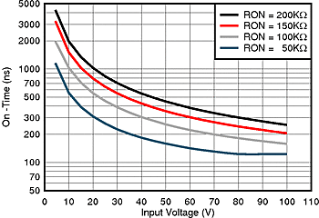
| TON Test 1 | VIN = 24 V, RON = 100 kΩ | 420 | 540 | 665 | ns | |
| TON Test 2 | VIN = 48 V, RON = 100 kΩ | 270 | ns | |||
| TON Test 3 | VIN = 8 V, RON = 100 kΩ | 1150 | 1325 | 1500 | ns | |
| TON Test 4 | VIN = 72V, RON = 150 kΩ | 285 | ns | |||
(1) All minimum and maximum limits are specified by correlating the electrical characteristics to process and temperature variations and applying statistical process control.
6.7 Typical Characteristics
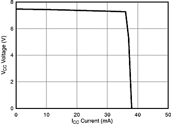
At TA = 25°C and applicable to LM5161 unless otherwise noted.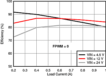
| VOUT = 3.3 V | RON = 110 kΩ | |
| FPWM = 0 |
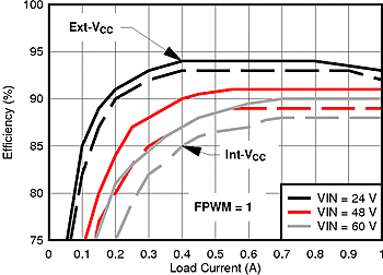
| VOUT = 12 V | RON = 402 kΩ | |
| FPWM = 0 | L = 100 µH |
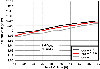
| VOUT = 12 V | RON = 300 kΩ | |
| FPWM = 1 | L = 100 µH |
| VIN = 48 V | ||
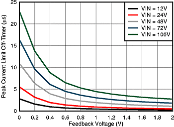
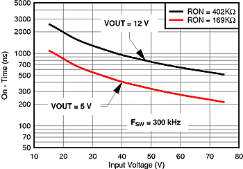
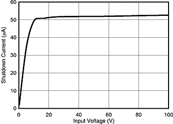
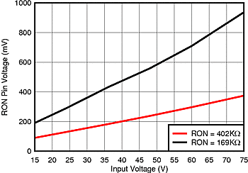
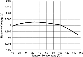
| VIN = 48 V | ||
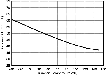
| VIN = 48 V | ||
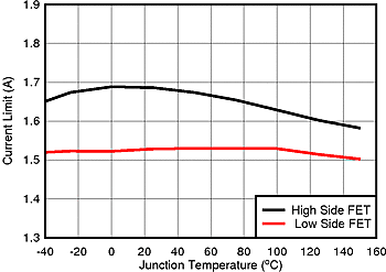
| VIN = 48 V | ||
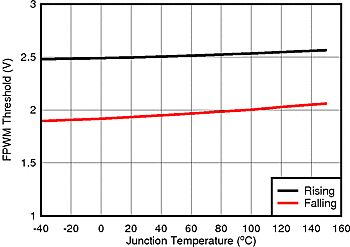
| VIN = 48 V | ||
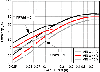
| VOUT = 5 V | RON = 169 kΩ | |
| L=47 µH |
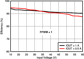
| VOUT = 12 V | RON = 402 kΩ | |
| FPWM = 1 | L = 100 µH |
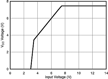
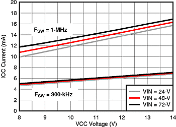
| IOUT = 1 A | FPWM = 0 | |
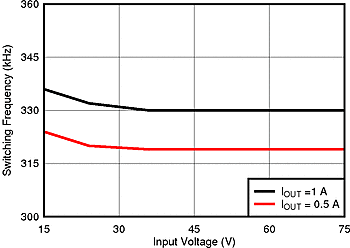
| VOUT = 12 V | ||
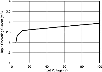
| VFB = 3 V | ||
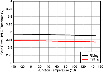
| VIN = 48 V | ||
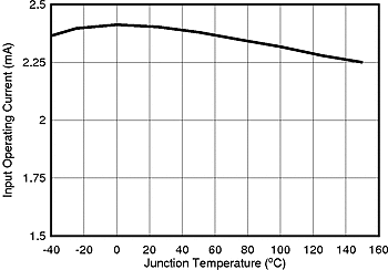
| VIN = 48 V | ||
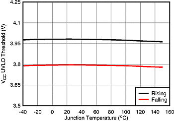
| VIN = 48 V | ||
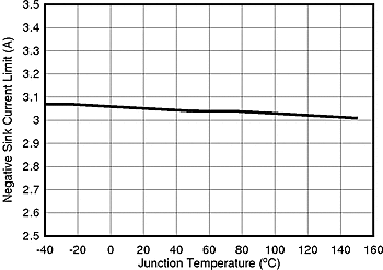
| VIN = 48 V | ||
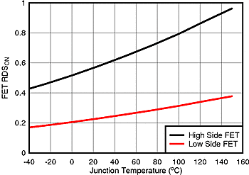
| ISW = 500 mA | VIN = 48 V | |