SNVSAU4C September 2018 – April 2024 LM5164
PRODUCTION DATA
- 1
- 1 Features
- 2 Applications
- 3 Description
- 4 Pin Configuration and Functions
- 5 Specifications
-
6 Detailed Description
- 6.1 Overview
- 6.2 Functional Block Diagram
- 6.3
Feature Description
- 6.3.1 Control Architecture
- 6.3.2 Internal VCC Regulator and Bootstrap Capacitor
- 6.3.3 Regulation Comparator
- 6.3.4 Internal Soft Start
- 6.3.5 On-Time Generator
- 6.3.6 Current Limit
- 6.3.7 N-Channel Buck Switch and Driver
- 6.3.8 Synchronous Rectifier
- 6.3.9 Enable/Undervoltage Lockout (EN/UVLO)
- 6.3.10 Power Good (PGOOD)
- 6.3.11 Thermal Protection
- 6.4 Device Functional Modes
- 7 Application and Implementation
- 8 Device and Documentation Support
- 9 Revision History
- 10Mechanical, Packaging, and Orderable Information
Package Options
Mechanical Data (Package|Pins)
- DDA|8
Thermal pad, mechanical data (Package|Pins)
- DDA|8
Orderable Information
6.3.9 Enable/Undervoltage Lockout (EN/UVLO)
The LM5164 contains a dual-level EN/UVLO circuit. When the EN/UVLO voltage is below 1.1 V (typical), the converter is in a low-current shutdown mode and the input quiescent current (IQ) is dropped down to 3 µA. When the voltage is greater than 1.1 V but less than 1.5 V (typical), the converter is in standby mode. In standby mode, the internal bias regulator is active while the control circuit is disabled. When the voltage exceeds the rising threshold of 1.5 V (typical), normal operation begins. Install a resistor divider from VIN to GND to set the minimum operating voltage of the regulator. Use Equation 13 and Equation 14 to calculate the input UVLO turnon and turnoff voltages, respectively.
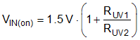
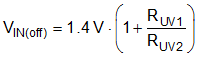
TI recommends selecting RUV1 in the range of 1 MΩ for most applications. A larger RUV1 consumes less DC current, which is mandatory if light-load efficiency is critical. If input UVLO is not required, the power-supply designer can either drive EN/UVLO as an enable input driven by a logic signal or connect it directly to VIN. If EN/UVLO is directly connected to VIN, the regulator begins switching as soon as the internal bias rails are active.