SNVSAU4C September 2018 – April 2024 LM5164
PRODUCTION DATA
- 1
- 1 Features
- 2 Applications
- 3 Description
- 4 Pin Configuration and Functions
- 5 Specifications
-
6 Detailed Description
- 6.1 Overview
- 6.2 Functional Block Diagram
- 6.3
Feature Description
- 6.3.1 Control Architecture
- 6.3.2 Internal VCC Regulator and Bootstrap Capacitor
- 6.3.3 Regulation Comparator
- 6.3.4 Internal Soft Start
- 6.3.5 On-Time Generator
- 6.3.6 Current Limit
- 6.3.7 N-Channel Buck Switch and Driver
- 6.3.8 Synchronous Rectifier
- 6.3.9 Enable/Undervoltage Lockout (EN/UVLO)
- 6.3.10 Power Good (PGOOD)
- 6.3.11 Thermal Protection
- 6.4 Device Functional Modes
- 7 Application and Implementation
- 8 Device and Documentation Support
- 9 Revision History
- 10Mechanical, Packaging, and Orderable Information
Package Options
Mechanical Data (Package|Pins)
- DDA|8
Thermal pad, mechanical data (Package|Pins)
- DDA|8
Orderable Information
6.3.3 Regulation Comparator
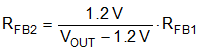
The feedback voltage at FB is compared to an internal 1.2-V reference. The LM5164 voltage regulation loop regulates the output voltage by maintaining the FB voltage equal to the internal reference voltage, VREF. A resistor divider programs the ratio from output voltage VOUT to FB.
For a target VOUT setpoint, use Equation 10 to calculate RFB2 based on the selected RFB1.
TI recommends selecting RFB1 in the range of 100 kΩ to 1 MΩ for most applications. A larger RFB1 consumes less DC current, which is mandatory if light-load efficiency is critical. RFB1 larger than 1 MΩ is not recommended as the feedback path becomes more susceptible to noise. It is important to route the feedback trace away from the noisy area of the PCB and keep the feedback resistors close to the FB pin.