SNVSAU4C September   2018  – April 2024 LM5164

PRODUCTION DATA  

  1.   1
  2. Features
  3. Applications
  4. Description
  5. Pin Configuration and Functions
  6. Specifications
    1. 5.1 Absolute Maximum Ratings
    2. 5.2 ESD Ratings
    3. 5.3 Recommended Operating Conditions
    4. 5.4 Thermal Information
    5. 5.5 Electrical Characteristics
    6. 5.6 Typical Characteristics
  7. Detailed Description
    1. 6.1 Overview
    2. 6.2 Functional Block Diagram
    3. 6.3 Feature Description
      1. 6.3.1  Control Architecture
      2. 6.3.2  Internal VCC Regulator and Bootstrap Capacitor
      3. 6.3.3  Regulation Comparator
      4. 6.3.4  Internal Soft Start
      5. 6.3.5  On-Time Generator
      6. 6.3.6  Current Limit
      7. 6.3.7  N-Channel Buck Switch and Driver
      8. 6.3.8  Synchronous Rectifier
      9. 6.3.9  Enable/Undervoltage Lockout (EN/UVLO)
      10. 6.3.10 Power Good (PGOOD)
      11. 6.3.11 Thermal Protection
    4. 6.4 Device Functional Modes
      1. 6.4.1 Shutdown Mode
      2. 6.4.2 Active Mode
      3. 6.4.3 Sleep Mode
  8. Application and Implementation
    1. 7.1 Application Information
    2. 7.2 Typical Application
      1. 7.2.1 Design Requirements
      2. 7.2.2 Detailed Design Procedure
        1. 7.2.2.1 Custom Design With WEBENCH® Tools
        2. 7.2.2.2 Switching Frequency (RRON)
        3. 7.2.2.3 Buck Inductor (LO)
        4. 7.2.2.4 Output Capacitor (COUT)
        5. 7.2.2.5 Input Capacitor (CIN)
        6. 7.2.2.6 Type-3 Ripple Network
      3. 7.2.3 Application Curves
    3. 7.3 Power Supply Recommendations
    4. 7.4 Layout
      1. 7.4.1 Layout Guidelines
        1. 7.4.1.1 Compact PCB Layout for EMI Reduction
        2. 7.4.1.2 Feedback Resistors
      2. 7.4.2 Layout Example
  9. Device and Documentation Support
    1. 8.1 Device Support
      1. 8.1.1 Third-Party Products Disclaimer
      2. 8.1.2 Development Support
        1. 8.1.2.1 Custom Design With WEBENCH® Tools
    2. 8.2 Documentation Support
      1. 8.2.1 Related Documentation
    3. 8.3 Receiving Notification of Documentation Updates
    4. 8.4 Support Resources
    5. 8.5 Trademarks
    6. 8.6 Electrostatic Discharge Caution
    7. 8.7 Glossary
  10. Revision History
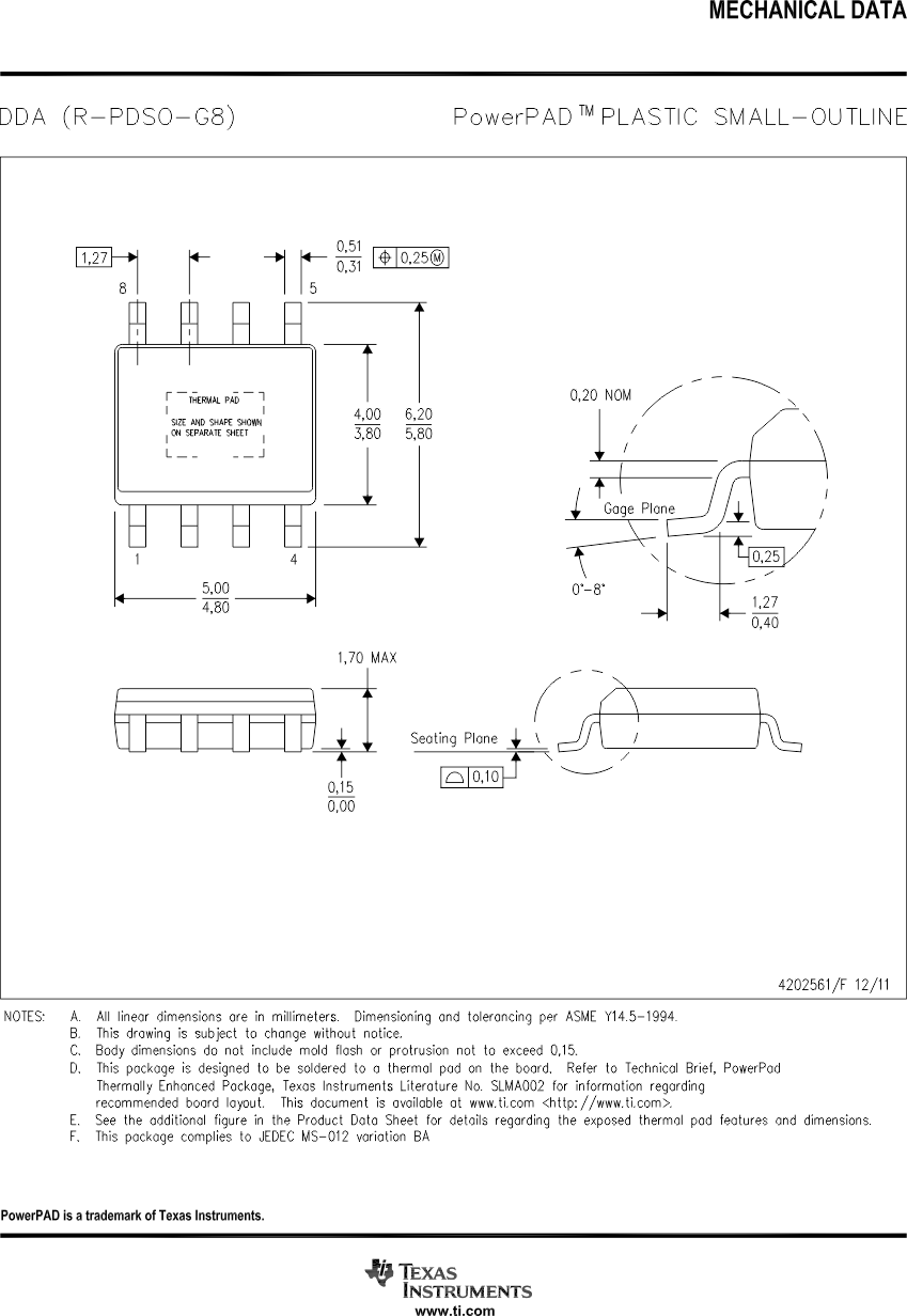
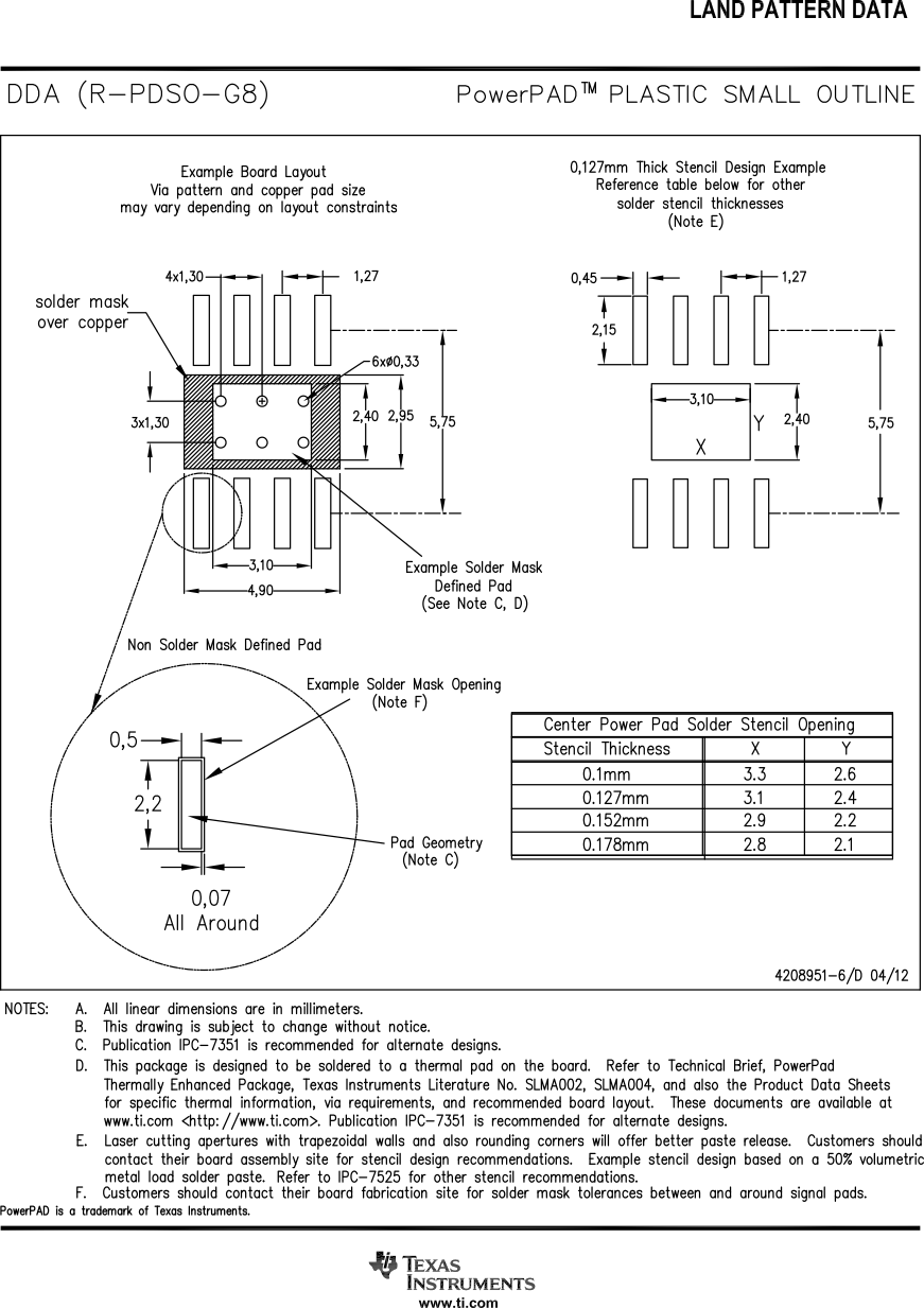
  11. 10Mechanical, Packaging, and Orderable Information

Package Options

Refer to the PDF data sheet for device specific package drawings

Mechanical Data (Package|Pins)
  • DDA|8
Thermal pad, mechanical data (Package|Pins)
Orderable Information

Mechanical, Packaging, and Orderable Information

The following pages include mechanical packaging and orderable information. This information is the most current data available for the designated devices. This data is subject to change without notice and revision of this document. For browser-based versions of this data sheet, refer to the left-hand navigation.

GUID-20220801-SS0I-GQ7W-7MQD-CLBWWQVR7RV5-low.gif
GUID-20230801-SS0I-B0FC-T7FG-HQ0JLG8K3PRL-low.svg
GUID-20220801-SS0I-QVXT-FMSS-FBX4CXP5F4RB-low.gif