SNVSBA0E February 2020 – October 2025 LM61480-Q1 , LM61495-Q1 , LM62460-Q1
PRODUCTION DATA
- 1
- 1 Features
- 2 Applications
- 3 Description
- 4 Device Comparison Table
- 5 Pin Configuration and Functions
- 6 Specifications
-
7 Detailed Description
- 7.1 Overview
- 7.2 Functional Block Diagram
- 7.3
Feature Description
- 7.3.1 Output Voltage Selection
- 7.3.2 Enable EN Pin and Use as VIN UVLO
- 7.3.3 SYNC/MODE Uses for Synchronization
- 7.3.4 Clock Locking
- 7.3.5 Adjustable Switching Frequency
- 7.3.6 RESET Output Operation
- 7.3.7 Internal LDO, VCC UVLO, and BIAS Input
- 7.3.8 Bootstrap Voltage and VCBOOT-UVLO (CBOOT Pin)
- 7.3.9 Adjustable SW Node Slew Rate
- 7.3.10 Spread Spectrum
- 7.3.11 Soft Start and Recovery From Dropout
- 7.3.12 Overcurrent and Short-Circuit Protection
- 7.3.13 Hiccup
- 7.3.14 Thermal Shutdown
- 7.4 Device Functional Modes
-
8 Application and Implementation
- 8.1 Application Information
- 8.2
Typical Application
- 8.2.1 Design Requirements
- 8.2.2
Detailed Design Procedure
- 8.2.2.1 Choosing the Switching Frequency
- 8.2.2.2 Setting the Output Voltage
- 8.2.2.3 Inductor Selection
- 8.2.2.4 Output Capacitor Selection
- 8.2.2.5 Input Capacitor Selection
- 8.2.2.6 BOOT Capacitor
- 8.2.2.7 BOOT Resistor
- 8.2.2.8 VCC
- 8.2.2.9 CFF and RFF Selection
- 8.2.2.10 RSPSP Selection
- 8.2.2.11 RT Selection
- 8.2.2.12 RMODE Selection
- 8.2.2.13 External UVLO
- 8.2.2.14 Maximum Ambient Temperature
- 8.2.3 Application Curves
- 8.3 Power Supply Recommendations
- 8.4 Layout
- 9 Device and Documentation Support
- 10Revision History
- 11Mechanical, Packaging, and Orderable Information
Package Options
Mechanical Data (Package|Pins)
- RPH|16
Thermal pad, mechanical data (Package|Pins)
- RPH|16
Orderable Information
8.2.3 Application Curves
Unless otherwise specified, the following conditions apply: device: LM61495-Q1, VIN = 13.5 V, TA = 25°C. Figure 8-1 shows the circuit, with the appropriate BOM from Table 8-4.

| VOUT = 5 V | FSW = 400 kHz | Auto mode |

| VOUT = 3.3 V | FSW = 400 kHz | Auto mode |

| VOUT = 5 V | FSW = 2.2 MHz | Auto mode |

| VOUT = 3.3 V | FSW = 2.2 MHz | Auto mode |
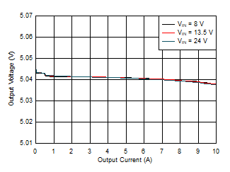
| VOUT = 5 V | FSW = 400 kHz | Auto mode |

| VOUT = 3.3 V | FSW = 400 kHz | Auto mode |

| VOUT = 5 V | FSW = 2.2 MHz | Auto mode |

| VOUT = 3.3 V | FSW = 2.2 MHz | Auto mode |

| VOUT = 5 V | FSW = 400 kHz | Auto mode |
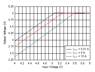
| VOUT = 5 V | FSW = 2.2 MHz | Auto mode |

| VOUT = 5 V | FSW = 400 kHz | Auto mode |
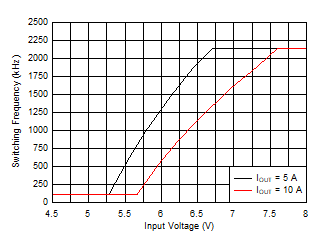
| VOUT = 5 V | FSW = 2.2 MHz | Auto mode |

| VOUT = 5 V | FSW = 2100 kHz | Auto mode |
| IOUT = 50 mA | VIN = 13.5 V |

| VOUT = 5 V | FSW = 2100 kHz | Auto mode |
| IOUT = 50 mA | VIN = 13.5 V |

| VOUT = 3.3 V | FSW = 2100 kHz | FPWM mode |
| IOUT = 3.25 A | VIN = 13.5 V |

| VOUT = 5 V | FSW = 2100 kHz | FPWM mode |
| IOUT = Short Circuit to 5 A | VIN = 13.5 V | |

| VOUT = 5 V | FSW = 400 kHz | Auto mode |
| IOUT = 10 mA to 10 A to 10 mA | VIN = 13.5 V | TR = TF = 1 µs |

| VOUT = 5 V | FSW = 400 kHz | Auto mode |
| IOUT = 2 A to 4 A to 2 A | VIN = 13.5 V | TR = TF = 1 µs |

| VOUT = 3.3 V | FSW = 400 kHz | Auto mode |
| IOUT = 10 mA to 10 A to 10 mA | VIN = 13.5 V | TR = TF = 1 µs |

| VOUT = 5 V | FSW = 2200 kHz | FPWM mode |
| IOUT = 10 mA to 10 A to 10 mA | VIN = 13.5 V | TR = TF = 1 µs |

| VOUT = 5 V | FSW = 2200 kHz | Auto mode |
| IOUT = 5 A to 10 A to 5 A | VIN = 13.5 V | TR = TF = 1 µs |

| VOUT = 5 V | FSW = 400 kHz | IOUT = 10 A |
| Frequency Tested: 30 MHz to 300 MHz | ||

| VOUT = 5 V | FSW = 400 kHz | IOUT = 10 A |
| Frequency Tested: 300 MHz to 1 GHz | ||


| VOUT = 5 V | FSW = 2.2 MHz | IOUT = 4 A |
| Frequency Tested: 30 MHz to 300 MHz | ||

| VOUT = 5 V | FSW = 2.2 MHz | IOUT = 4 A |
| Frequency Tested: 300 MHz to 1 GHz | ||
 Figure 8-57 Recommended
Input EMI Filter
| VOUT = 5 V | FSW = 400 kHz | FPWM mode |

| VOUT = 3.3 V | FSW = 400 kHz | FPWM mode |

| VOUT = 5 V | FSW = 2.2 MHz | FPWM mode |

| VOUT = 3.3 V | FSW = 2.2 MHz | FPWM mode |

| VOUT = 5 V | FSW = 400 kHz | FPWM mode |

| VOUT = 3.3 V | FSW = 400 kHz | FPWM mode |

| VOUT = 5 V | FSW = 2.2 MHz | FPWM mode |

| VOUT = 3.3 V | FSW = 2.2 MHz | FPWM mode |
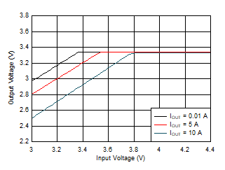
| VOUT = 3.3 V | FSW = 400 kHz | Auto mode |
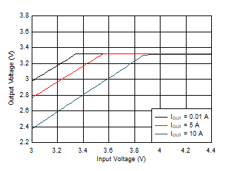
| VOUT = 3.3 V | FSW = 2.2 MHz | Auto mode |

| VOUT = 3.3 V | FSW = 400 kHz | Auto mode |
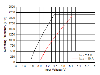
| VOUT = 3.3 V | FSW = 2.2 MHz | Auto mode |

| VOUT = 5 V | FSW = 2100 kHz | FPWM mode |
| IOUT = 50 mA | VIN = 13.5 V |

| VOUT = 5 V | FSW = 2100 kHz | FPWM mode |
| IOUT = 50 mA | VIN = 13.5 V |

| VOUT = 5 V | FSW = 2100 kHz | FPWM mode |
| IOUT = 5 A to Short Circuit | VIN = 13.5 V |

| VOUT = 5 V | FSW = 2100 kHz | FPWM mode |
| IOUT = 4 A | VIN = 13.5 V to 4 V to 13.5 V | |

| VOUT = 5 V | FSW = 400 kHz | FPWM mode |
| IOUT = 10 mA to 10 A to 10 mA | VIN = 13.5 V | TR = TF = 1 µs |

| VOUT = 5 V | FSW = 400 kHz | Auto mode |
| IOUT = 5 A to 10 A to 5 A | VIN = 13.5 V | TR = TF = 1 µs |

| VOUT = 3.3 V | FSW = 400 kHz | Auto mode |
| IOUT = 5 A to 10 A to 5 A | VIN = 13.5 V | TR = TF = 1 µs |

| VOUT = 5 V | FSW = 2200 kHz | Auto mode |
| IOUT = 2 A to 4 A to 2 A | VIN = 13.5 V | TR = TF = 1 µs |

| VOUT = 5 V | FSW = 400 kHz | IOUT = 10 A |
| Frequency Tested: 150 kHz to 30 MHz | ||

| VOUT = 5 V | FSW = 400 kHz | IOUT = 10 A |
| Frequency Tested: 30 MHz to 300 MHz | ||

| VOUT = 5 V | FSW = 400 kHz | IOUT = 10 A |
| Frequency Tested: 300 MHz to 1 GHz | ||

| VOUT = 5 V | FSW = 2.2 MHz | IOUT = 4 A |
| Frequency Tested: 150 kHz to 30 MHz | ||

| VOUT = 5 V | FSW = 2.2 MHz | IOUT = 4 A |
| Frequency Tested: 30 MHz to 300 MHz | ||

| VOUT = 5 V | FSW = 2.2 MHz | IOUT = 4 A |
| Frequency Tested: 300 MHz to 1 GHz | ||
Table 8-4 BOM for Typical Application
Curves
| VOUT | FREQUENCY | RFBB | COUT | CIN + CHF | L | CFF |
|---|---|---|---|---|---|---|
| 3.3 V | 400 kHz | 43.2 kΩ | 4 × 47 µF + 100 µF electrolytic + 2 × 2.2 µF | 4 × 10 µF + 2 × 470 nF + 100 µF electrolytic | 2.4 µH (744325240) | 22 pF |
| 3.3 V | 2200 kHz | 43.2 kΩ | 2 × 47 µF + 100 µF electrolytic + 2 × 2.2 µF | 2 × 10 µF + 2 × 470 nF + 100 µF electrolytic | 0.68 µH (744373460068) | 10 pF |
| 5 V | 400 kHz | 24.9 kΩ | 4 × 47 µF + 100 µF electrolytic + 2 × 2.2 µF | 4 × 10 µF + 2 × 470 nF + 100 µF electrolytic | 2.4 µH (744325240) | 22 pF |
| 5 V | 2200 kHz | 24.9 kΩ | 2 × 47 µF + 100 µF electrolytic + 2 × 2.2 µF | 2 × 10 µF + 2 × 470 nF + 100 µF electrolytic | 0.68 µH (744373460068) | 10 pF |