SNOSD62 June 2017 LM741-MIL
PRODUCTION DATA.
- 1 Features
- 2 Applications
- 3 Description
- 4 Revision History
- 5 Pin Configuration and Functions
- 6 Specifications
- 7 Detailed Description
- 8 Application and Implementation
- 9 Power Supply Recommendations
- 10Layout
- 11Device and Documentation Support
- 12Mechanical, Packaging, and Orderable Information
Package Options
Mechanical Data (Package|Pins)
Thermal pad, mechanical data (Package|Pins)
Orderable Information
8 Application and Implementation
NOTE
Information in the following applications sections is not part of the TI component specification, and TI does not warrant its accuracy or completeness. TI’s customers are responsible for determining suitability of components for their purposes. Customers should validate and test their design implementation to confirm system functionality.
8.1 Application Information
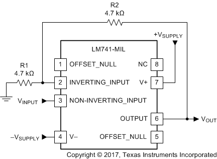
The LM741-MIL is a general-purpose amplifier than can be used in a variety of applications and configurations. One common configuration is in a non-inverting amplifier configuration. In this configuration, the output signal is in phase with the input (not inverted as in the inverting amplifier configuration), the input impedance of the amplifier is high, and the output impedance is low. The characteristics of the input and output impedance is beneficial for applications that require isolation between the input and output. No significant loading will occur from the previous stage before the amplifier. The gain of the system is set accordingly so the output signal is a factor larger than the input signal.
8.2 Typical Application
 Figure 1. LM741-MIL Noninverting Amplifier Circuit
8.2.1 Design Requirements
As shown in Figure 1, the signal is applied to the noninverting input of the LM741-MIL. The gain of the system is determined by the feedback resistor and input resistor connected to the inverting input. The gain can be calculated by Equation 1:
The gain is set to 2 for this application. R1 and R2 are 4.7-kΩ resistors with 5% tolerance.
8.2.2 Detailed Design Procedure
The LM741-MIL can be operated in either single supply or dual supply. This application is configured for dual supply with the supply rails at ±15 V. The input signal is connected to a function generator. A 1-VPP, 10-kHz sine wave was used as the signal input. 5% tolerance resistors were used, but if the application requires an accurate gain response, use 1% tolerance resistors.
8.2.3 Application Curve
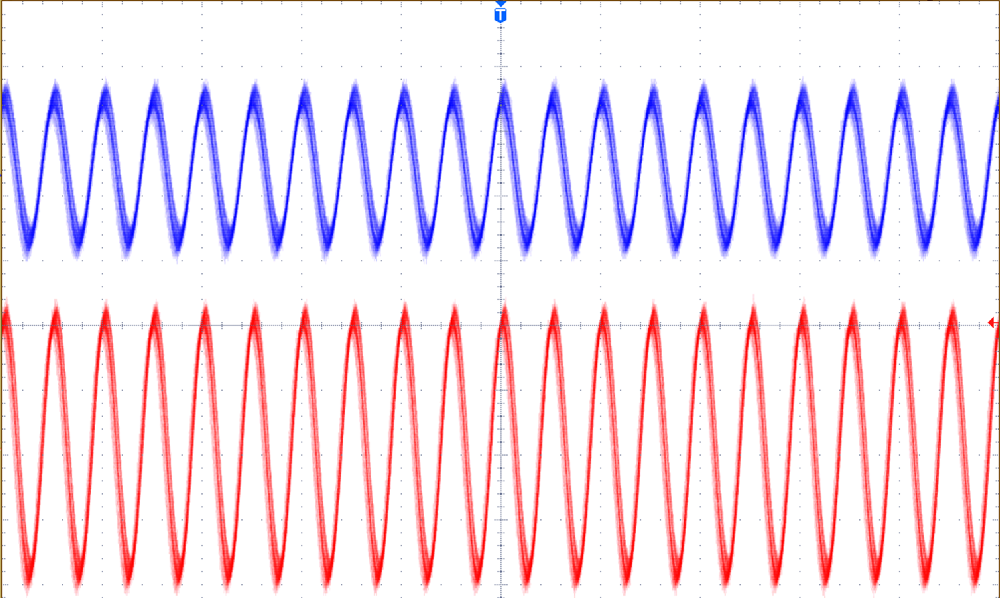
The waveforms in Figure 2 show the input and output signals of the LM741-MIL non-inverting amplifier circuit. The blue waveform (top) shows the input signal, while the red waveform (bottom) shows the output signal. The input signal is 1.06 VP-P and the output signal is 1.94 VP-P. With the 4.7-kΩ resistors, the theoretical gain of the system is 2. Due to the 5% tolerance, the gain of the system including the tolerance is 1.992. The gain of the system when measured from the mean amplitude values on the oscilloscope was 1.83.
 Figure 2. Waveforms for LM741-MIL Non-inverting Amplifier Circuit