SNOSDD9 December 2022 LM7481
PRODUCTION DATA
- 1 Features
- 2 Applications
- 3 Description
- 4 Revision History
- 5 Pin Configuration and Functions
- 6 Specifications
- 7 Parameter Measurement Information
- 8 Detailed Description
-
9 Application and Implementation
- 9.1 Application Information
- 9.2 Typical 12-V Reverse Battery Protection Application
- 9.3 Do's and Don'ts
- 9.4 Power Supply Recommendations
- 9.5 Layout
- 10Device and Documentation Support
- 11Mechanical, Packaging, and Orderable Information
Package Options
Mechanical Data (Package|Pins)
- DRR|12
Thermal pad, mechanical data (Package|Pins)
- DRR|12
Orderable Information
8.3.1 Charge Pump
The charge pump supplies the voltage necessary to drive the external N-channel MOSFET. An external charge pump capacitor is placed between CAP and VS pins to provide energy to turn on the external MOSFET. In order for the charge pump to supply current to the external capacitor the EN/UVLO pin voltage must be above the specified input high threshold, V(ENR). When enabled, the charge pump sources a charging current of 3.8-mA typical. If EN/UVLO pin is pulled low, then the charge pump remains disabled. To ensure that the external MOSFET can be driven above its specified threshold voltage, the CAP to VS voltage must be above the undervoltage lockout threshold, typically 6.6 V, before the internal gate driver is enabled. Use Equation 1 to calculate the initial gate driver enable delay.
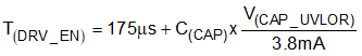
where
- C(CAP) is the charge pump capacitance connected across VS and CAP pins
- V(CAP_UVLOR) = 6.6 V (typical)
To remove any chatter on the gate drive approximately 1 V of hysteresis is added to the VCAP undervoltage lockout. The charge pump remains enabled until the CAP to VS voltage reaches 13.2 V, typically, at which point the charge pump is disabled decreasing the current draw on the VS pin. The charge pump remains disabled until the CAP to VS voltage is below to 12.2 V typically at which point the charge pump is enabled. The voltage between CAP and VS continue to charge and discharge between 12.2 V and 13.2 V as shown in Figure 8-1. By enabling and disabling the charge pump, the operating quiescent current of the LM74810 is reduced. When the charge pump is disabled it sinks 15 µA.
 Figure 8-1 Charge Pump Operation