SNVS420D November 2008 – May 2018 LM7705
PRODUCTION DATA.
- 1 Features
- 2 Applications
- 3 Description
- 4 Revision History
- 5 Pin Configuration and Functions
- 6 Specifications
- 7 Detailed Description
- 8 Application and Implementation
- 9 Power Supply Recommendations
- 10Layout
- 11Device and Documentation Support
- 12Mechanical, Packaging, and Orderable Information
Package Options
Mechanical Data (Package|Pins)
- DGK|8
Thermal pad, mechanical data (Package|Pins)
Orderable Information
8.1.3 Charge Pump Theory
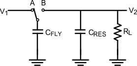
This section uses a simplified but realistic equivalent circuit that represents the basic function of the charge pump. The schematic is given in Figure 30.
 Figure 30. Charge Pump
 When the switch is in position A, capacitor CFLY will charge to voltage V1. The total charge on capacitor CFLY is Q1 = CFLY × V 1. The switch then moves to position B, discharging CFLY to voltage V2. After this discharge, the charge on CFLY will be Q2 = CFLY × V2. The charge has been transferred from the source V1 to the output V2. The amount of charge transferred is:

When the switch changes between A and B at a frequency f, the charge transfer per unit time, or current is:

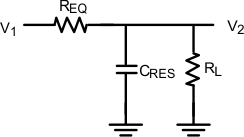
The switched capacitor network can be replaced by an equivalent resistor, as indicated in Figure 31.
 Figure 31. Switched Capacitor Equivalent Circuit
 The value of this resistor is dependent on both the capacitor value and the switching frequency as given in Equation 3

The value for REQ can be calculated from Equation 3 and is given in Equation 4

Equation 4 show that the value for the resistance at an increased internal switching frequency, allows a lower value for the used capacitor.