SNVS420D November 2008 – May 2018 LM7705
PRODUCTION DATA.
- 1 Features
- 2 Applications
- 3 Description
- 4 Revision History
- 5 Pin Configuration and Functions
- 6 Specifications
- 7 Detailed Description
- 8 Application and Implementation
- 9 Power Supply Recommendations
- 10Layout
- 11Device and Documentation Support
- 12Mechanical, Packaging, and Orderable Information
Package Options
Mechanical Data (Package|Pins)
- DGK|8
Thermal pad, mechanical data (Package|Pins)
Orderable Information
7.4.1 General Amplifier Application
This section will discuss a general DC coupled amplifier application. First, one of the limitations of a DC coupled amplifier is discussed. This is illustrated with two application examples. A solution is a given for solving this limitation by using the LM7705.
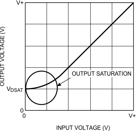
Due to the architecture of the output stage of general amplifiers, the output transistors will saturate. As a result, the output of a general purpose op amp can only swing to a few 100 mV of the supply rails. Amplifiers using CMOS technology do have a lower output saturation voltage. This is illustrated in Figure 22. For example, Texas Instruments' LM7332 can swing to 200 mV to the negative rail, for a 10-kΩ load, over all temperatures.
 Figure 22. Limitation of the Output of an Amplifier
 The introduction of operational amplifiers with output rail-to-rail drive capabilities is a strong improvement and the (output) performance of op amps is for many applications no longer a limiting factor. For example, Texas Instruments' LMP7701 (a typical rail-to-rail op amp), has an output drive capability of only 50 mV over all temperatures for a 10-kΩ load resistance. This is close to the lower supply voltage rail.
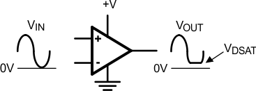
However, for true zero output applications with a single supply, the saturation voltage of the output stage is still a limiting factor. This limitation has a negative impact on the functionality of true zero output applications. This is illustrated in Figure 23.
 Figure 23. Output Limitation for Single-Supply True Zero Output Application
 In the One-Stage, Single-Supply True Zero Amplifier section, two applications will be discussed, showing the limitations of the output stage of an op amp in a single supply configuration:
- A single stage true zero amplifier, with a 12-bit ADC back end.
- A dual stage true zero amplifier, with a 12-bit ADC back end.