SNVS420D November 2008 – May 2018 LM7705
PRODUCTION DATA.
- 1 Features
- 2 Applications
- 3 Description
- 4 Revision History
- 5 Pin Configuration and Functions
- 6 Specifications
- 7 Detailed Description
- 8 Application and Implementation
- 9 Power Supply Recommendations
- 10Layout
- 11Device and Documentation Support
- 12Mechanical, Packaging, and Orderable Information
Package Options
Mechanical Data (Package|Pins)
- DGK|8
Thermal pad, mechanical data (Package|Pins)
- DGK|8
Orderable Information
7.4.1.1 One-Stage, Single-Supply True Zero Amplifier
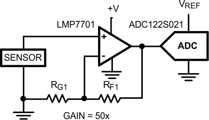
This application shows a sensor with a DC output signal, amplified by a single supply op amp. The output voltage of the op amp is converted to the digital domain using an Analog to Digital Converter (ADC). Figure 24 shows the basic set-up of this application.
 Figure 24. Sensor With DC Output and a Single-Supply Op Amp
 The sensor has a DC output signal that is amplified by the op amp. For an optimal signal-to-noise ratio, the output voltage swing of the op amp must be matched to the input voltage range of the Analog to Digital Converter (ADC). For the high side of the range this can be done by adjusting the gain of the op amp. However, the low side of the range cannot be adjusted and is affected by the output swing of the op amp.
Example:
Assume the output voltage range of the sensor is 0 to 90 mV. The available op amp is a LMP7701, using a 0/+5-V supply voltage, having an output drive of 50 mV from both rails. This results in an output range of 50 mV to 4.95V.
Select two resistors values for RG1 and RF1 that result in a gain of 50x. The output of the LMP7701 must swing from 0 mV to 4.5 V. The higher value is no problem, however the lower swing is limited by the output of the LM7701 and won’t go below 50 mV instead of the desired 0 V, causing a non-linearity in the sensor reading. When using a 12-bit ADC, and a reference voltage of 5 V (having an ADC step size of approximate 1.2 mV), the output saturation results in a loss of the lower 40 quantization levels of the ADCs dynamic range.