SNVS052E September   1999  – April 2016 LM809 , LM810

PRODUCTION DATA.  

  1. Features
  2. Applications
  3. Description
  4. Revision History
  5. Pin Configuration and Functions
  6. Specifications
    1. 6.1 Absolute Maximum Ratings
    2. 6.2 ESD Ratings
    3. 6.3 Recommended Operating Conditions
    4. 6.4 Thermal Information
    5. 6.5 Electrical Characteristics
    6. 6.6 Typical Characteristics
  7. Detailed Description
    1. 7.1 Overview
    2. 7.2 Functional Block Diagram
    3. 7.3 Feature Description
      1. 7.3.1 Benefits of Precision Reset Thresholds
        1. 7.3.1.1 Ensuring a Valid Reset Output Down to VCC = 0 V
        2. 7.3.1.2 Negative-Going VCC Transients
        3. 7.3.1.3 Interfacing to µPs with Bidirectional Reset Pins
    4. 7.4 Device Functional Modes
      1. 7.4.1 VCC Supply Voltage Low
      2. 7.4.2 VCC Supply Voltage High
  8. Application and Implementation
    1. 8.1 Application Information
    2. 8.2 Typical Application
      1. 8.2.1 Design Requirements
      2. 8.2.2 Detailed Design Procedure
      3. 8.2.3 Application Curve
  9. Power Supply Recommendations
  10. 10Layout
    1. 10.1 Layout Guidelines
    2. 10.2 Layout Example
  11. 11Device and Documentation Support
    1. 11.1 Related Links
    2. 11.2 Community Resources
    3. 11.3 Trademarks
    4. 11.4 Electrostatic Discharge Caution
    5. 11.5 Glossary
  12. 12Mechanical, Packaging, and Orderable Information

Package Options

Mechanical Data (Package|Pins)
Thermal pad, mechanical data (Package|Pins)
Orderable Information

10 Layout

10.1 Layout Guidelines

Place the input capacitor as close as possible to the IC.

10.2 Layout Example
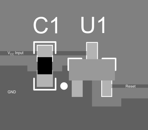
LM809 LM810 layout_snvs052.gif Figure 12. Layout Example