SNAS393D March 2007 – November 2016 LME49720
PRODUCTION DATA.
- 1 Features
- 2 Applications
- 3 Description
- 4 Revision History
- 5 Device Comparison Table
- 6 Pin Configuration and Functions
- 7 Specifications
- 8 Parameter Measurement Information
- 9 Detailed Description
- 10Application and Implementation
- 11Power Supply Recommendations
- 12Layout
- 13Device and Documentation Support
- 14Mechanical, Packaging, and Orderable Information
Package Options
Mechanical Data (Package|Pins)
Thermal pad, mechanical data (Package|Pins)
Orderable Information
8 Parameter Measurement Information
All parameters are measured according to the conditions described in the Specifications section.
8.1 Distortion Measurements
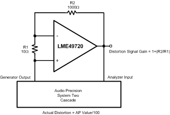
The vanishingly low residual distortion produced by LME49720 is below the capabilities of all commercially available equipment. This makes distortion measurements just slightly more difficult than simply connecting a distortion meter to the amplifier’s inputs and outputs. The solution, however, is quite simple: an additional resistor. Adding this resistor extends the resolution of the distortion measurement equipment.
The LME49720’s low residual distortion is an input referred internal error. As shown in Figure 109, adding the 10Ω resistor connected between the amplifier’s inverting and non-inverting inputs changes the amplifier’s noise gain. The result is that the error signal (distortion) is amplified by a factor of 101. Although the amplifier’s closed-loop gain is unaltered, the feedback available to correct distortion errors is reduced by 101, which means that measurement resolution increases by 101. To ensure minimum effects on distortion measurements, keep the value of R1 low as shown in Figure 109.
This technique is verified by duplicating the measurements with high closed loop gain and/or making the measurements at high frequencies. Doing so produces distortion components that are within the measurement equipment’s capabilities. This datasheet’s THD+N and IMD values were generated using the above described circuit connected to an Audio Precision System Two Cascade.
 Figure 109. THD+N and IMD Distortion Test Circuit

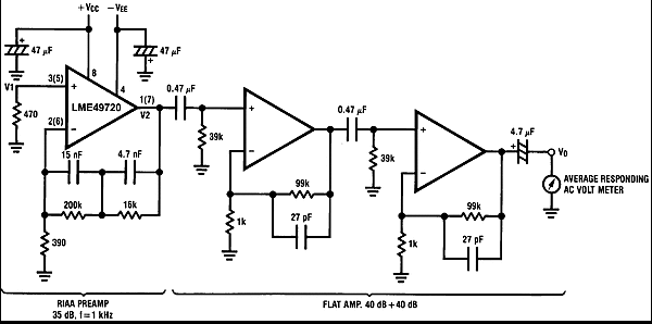
Total Gain: 115 dB @F = 1 kHz
Input Referred Noise Voltage: En = V0/560,000 (V)