SNLS531B April   2016  – June 2018 LMH0324

PRODUCTION DATA.  

  1. Features
  2. Applications
  3. Description
    1.     Device Images
      1.      Simplified Block Diagram
  4. Revision History
  5. Pin Configuration and Functions
    1.     Pin Functions
  6. Specifications
    1. 6.1 Absolute Maximum Ratings
    2. 6.2 ESD Ratings
    3. 6.3 Recommended Operating Conditions
    4. 6.4 Thermal Information
    5. 6.5 Electrical Characteristics
    6. 6.6 Recommended SMBus Interface AC Timing Specifications
    7. 6.7 Serial Parallel Interface (SPI) AC Timing Specifications
    8. 6.8 Typical Characteristics
  7. Detailed Description
    1. 7.1 Overview
    2. 7.2 Functional Block Diagram
    3. 7.3 Feature Description
      1. 7.3.1 4-Level Input Configuration Pins
      2. 7.3.2 Carrier Detect
      3. 7.3.3 Adaptive Cable Equalizer
      4. 7.3.4 Launch Amplitude
      5. 7.3.5 Input-Output Mux Selection
      6. 7.3.6 Output Function Control
      7. 7.3.7 Output Driver Amplitude and De-Emphasis Control
      8. 7.3.8 Additional Programmability
        1. 7.3.8.1 Cable Length Indicator (CLI)
        2. 7.3.8.2 Digital MUTEREF
    4. 7.4 Device Functional Modes
      1. 7.4.1 System Management Bus (SMBus) Mode
        1. 7.4.1.1 SMBus Read and Write Transactions
          1. 7.4.1.1.1 SMBus Write Operation Format
          2. 7.4.1.1.2 SMBus Read Operation Format
      2. 7.4.2 Serial Peripheral Interface (SPI) Mode
        1. 7.4.2.1 SPI Read and Write Transactions
          1. 7.4.2.1.1 SPI Write Transaction Format
          2. 7.4.2.1.2 SPI Read Transaction Format
        2. 7.4.2.2 SPI Daisy Chain
    5. 7.5 LMH0324 Register Map
      1. 7.5.1 Share Register Page
      2. 7.5.2 CableEQ/Drivers Register Page
  8. Application and Implementation
    1. 8.1 Application Information
      1. 8.1.1 General Guidance for SMPTE Applications
    2. 8.2 Typical Application
      1. 8.2.1 Design Requirements
      2. 8.2.2 Detailed Design Procedure
      3. 8.2.3 Recommended VOD and DE Register Settings
      4. 8.2.4 Application Performance Plots
  9. Power Supply Recommendations
  10. 10Layout
    1. 10.1 Layout Guidelines
    2. 10.2 Layout Example
  11. 11Device and Documentation Support
    1. 11.1 Receiving Notification of Documentation Updates
    2. 11.2 Community Resources
    3. 11.3 Trademarks
    4. 11.4 Electrostatic Discharge Caution
    5. 11.5 Glossary
  12. 12Mechanical, Packaging, and Orderable Information

Package Options

Refer to the PDF data sheet for device specific package drawings

Mechanical Data (Package|Pins)
  • RTW|24
Thermal pad, mechanical data (Package|Pins)
Orderable Information

Application Performance Plots

The LMH0324 performance was measured with the test setups shown in Figure 17.

LMH0324 app_test_setup_diagram_IN0.gifFigure 17. Test Setup for LMH0324 Cable Equalizer (IN0+)

The eye diagrams in this subsection show how the LMH0324 improves overall signal integrity in the data path when different cable lengths are used at IN0+.
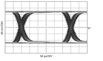
LMH0324 lmh1214_3gbps_150m.gifFigure 18. 2.97 Gbps, CC = 150 m Belden 1694A
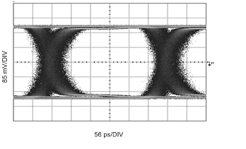
LMH0324 lmh1214_3gbps_200m.gifFigure 19. 2.97 Gbps, CC = 200 m Belden 1694A
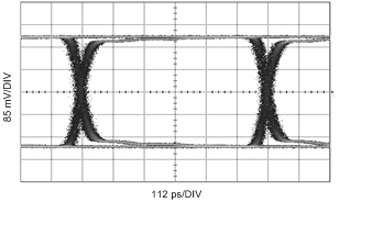
LMH0324 lmh1214_hd_200m.gifFigure 20. 1.485 Gbps, CC = 200 m Belden 1694A
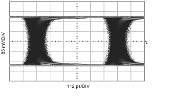
LMH0324 lmh1214_hd_280m.gifFigure 21. 1.485 Gbps, CC = 280 m Belden 1694A
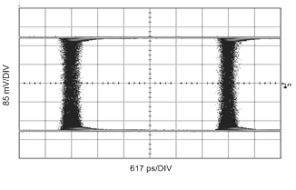
LMH0324 lmh1214_270mbps_sd_400m.gifFigure 22. 270 Mbps, CC = 400 m Belden 1694A
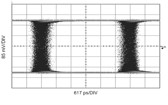
LMH0324 lmh1214_sd_600m.gifFigure 23. 270 Mbps, CC = 600 m Belden 1694A