SNLS289D April 2008 – September 2015 LMH1982
PRODUCTION DATA.
- 1 Features
- 2 Applications
- 3 Description
- 4 Revision History
- 5 Pin Configuration and Functions
- 6 Specifications
-
7 Detailed Description
- 7.1 Overview
- 7.2 Functional Block Diagram
- 7.3 Feature Description
- 7.4 Device Functional Modes
- 7.5 Programming
- 7.6
Register Maps
- 7.6.1
I2C Interface Control Register Definitions
- 7.6.1.1 Genlock and Input Reference Control Registers
- 7.6.1.2 Genlock Status And Lock Control Register
- 7.6.1.3 Input Control Register
- 7.6.1.4 PLL 1 Divider Register
- 7.6.1.5 PLL 4 Charge Pump Current Control Register
- 7.6.1.6 Output Clock and TOF Control Register
- 7.6.1.7 TOF Configuration Registers
- 7.6.1.8 PLL 1, 2, 3 Charge Pump Current Control Registers
- 7.6.1.9 Reserved Registers
- 7.6.1
I2C Interface Control Register Definitions
-
8 Application and Implementation
- 8.1
Application Information
- 8.1.1 148.35 MHz PLL Initialization Sequence
- 8.1.2 Enabling Genlock Mode
- 8.1.3 Output Disturbance While Output Alignment Mode Enabled
- 8.1.4 Evaluating the LMH1982
- 8.1.5 Input Reference
- 8.1.6 Output Clocks and TOF
- 8.1.7 Reference And Pll Lock Status
- 8.1.8 Loop Response
- 8.2 Typical Applications
- 8.1
Application Information
- 9 Power Supply Recommendations
- 10Layout
- 11Device and Documentation Support
- 12Mechanical, Packaging, and Orderable Information
Package Options
Mechanical Data (Package|Pins)
- RTV|32
Thermal pad, mechanical data (Package|Pins)
- RTV|32
Orderable Information
1 Features
-
Two Simultaneous LVDS Output Clocks with Selectable Frequencies and Hi-Z Capability:
- SD Clock: 27 MHz or 67.5 MHz
- HD Clock: 74.25 MHz, 74.25/1.001 MHz,
148.5 MHz or 148.5/1.001 MHz
- Low-Jitter Output Clocks May Be Directly Connected to an FPGA Serializer to Meet SMPTE SDI Jitter Specifications
- Top of Frame (TOF) Pulse with Programmable Output Format Timing and Hi-Z Capability
- Two reference ports (A and B) With H and V Sync Inputs
- Supports Cross-Locking of Input and Output Timing
- External Loop Filter Allows Control of Loop Bandwidth, Jitter Transfer, and Lock Time Characteristics
- Free Run or Holdover Operation on Loss of Reference
- User-Defined Free Run Control Voltage Input
- I2C Interface and Control Registers
- 3.3-V and 2.5-V Supplies
2 Applications
- Video Genlock and Synchronization
- FPGA SDI SerDes Recovered Clock Generation
- Triple Rate 3G/HD/SD-SDI SerDes
- Video Capture, Conversion, Editing and Distribution
- Video Displays and Projectors
- Broadcast and Professional Video Equipment
3 Description
The LMH1982 device is a multi-rate video clock generator ideal for use in a wide range of 3-Gbps (3G), high-definition (HD), and standard-definition (SD) video applications, such as video synchronization, serial digital interface (SDI) serializer and deserializer (SerDes), video conversion, video editing, and other broadcast and professional video systems.
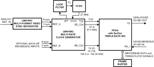
The LMH1982 can generate two simultaneous SD and HD clocks and a Top of Frame (TOF) pulse. In genlock mode, the device's phase locked loops (PLLs) can synchronize the output signals to H sync and V sync input signals applied to either of the reference ports. The input reference can have analog timing from Texas Instrument's LMH1981 multi-format video sync separator or digital timing from an SDI deserializer and should conform to the major SD and HD standards. When a loss of reference occurs, the device can default to free run operation where the output timing accuracy will be determined by the external bias on the free run control voltage input.
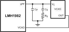
The LMH1982 can replace discrete PLLs and field-programmable gate array (FPGA) PLLs with multiple voltage controlled crystal oscillators (VCXOs). Only one 27.0000 MHz VCXO and loop filter are externally required for genlock mode. The external loop filter as well as programmable PLL parameters can provide narrow loop bandwidths to minimize jitter transfer. HD clock output jitter as low as 40 ps peak-to-peak can help designers using FPGA SerDes meet stringent SDI output jitter specifications.
The LMH1982 is offered in a space-saving 5 mm x 5 mm 32-pin WQFN package and provides low total power consumption of about 250 mW (typical).
Device Information(1)
| PART NUMBER | PACKAGE | BODY SIZE (NOM) |
|---|---|---|
| LMH1982 | WQFN (32) | 5.00 mm × 5.00 mm |
- For all available packages, see the orderable addendum at the end of the data sheet.
Typical Genlock Application

Typical Loop Filter Topology
